
Spoiler alert!
Don’t read any further unless you have gotten your design working for part two of tutorial 18. Well, at least the spirit of tutorial 18 is that you should really try to work it out on your own. This section will walk through some code examples in detail.
The literal implementation
You can go to the block diagram and just literally code everything that appears there. First we have the module declaration:
`timescale 1ns/1ns
module i2s_receive2a
  (
   input sck,
   input ws,
   input sd,
   output reg [31:0] data_left,
   output reg [31:0] data_right
   );
Next, we need to implement the two flip-flops which delay the WS signal by a clock. The part of the diagram that implements this is shown to the right.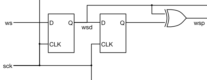 We will of course need two register values. One is called wsd, presumably for WS delayed. The second has no name in the figure and I just called it wsdd, for wsd delayed. I have also chosen to initialize wsd to zero. The code for this is really quite simple.
  reg wsd = 0;
  always @(posedge sck)
    wsd <= ws;

  reg wsdd;
  always @(posedge sck)
    wsdd <= wsd;
We also need a combinational XOR of wsd and wsdd and call that wsp. I do that like this:
wire wsp = wsd ^ wsdd;This uses the Verilog exclusive OR operator ^. We could also write it like this:
wire wsp = wsd != wsdd;This might be a little more expressive of our intent. We want a single clock pulse when the two signals are different. Ne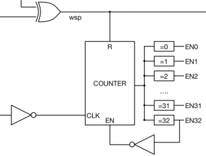 xt, we see that we need 32 enable signals for the flip-flops that capture the SD data input. Actually, if you look at the counter, you see that we need an additional one for when the counter is 32 to keep it from counting further.
Let’s declare those:
wire en0; wire en1; wire en2;...wire en31; wire en32;
Next, we’ll focus on the counter. It needs to count from zero to 32. We declare this to be a 6-bit register. Remember, six bits are needed to represent 0 to 32. Here is the counter. Also notice that it is clocked on the negative edge of SCK:
  reg [5:0] counter;
  always @(negedge sck)
    if (wsp)
      counter <= 0;
    else if (!en32)
      counter <= counter+1;
Then we need to also assign to the enable signals. Here is that code:
assign en0 = counter == 0; assign en1 = counter == 1; assign en2 = counter == 2;...assign en31 = counter == 31; assign en32 = counter == 32;
Next, let’s focus on the register that captures the data. In the previous example, the register was called shift. We will stick with that name, even though it’s no longer technically a shift register. It still kind of functions that way, so I think the name still makes sense. 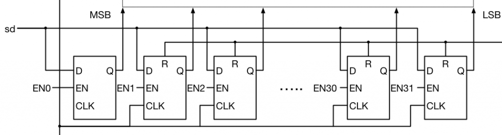 Notice that EN0 enables the most significant bit to be written. and EN31 enables the least significant bit. That means we naturally want the MSB of shift to be bit zero and the LSB of shift to be bit 31. So we declare shift as follows.
reg [0:31] shift;Also, notice that bit zero is different from the other bits. It has no reset input while the others do. Let’s code that bit first:
always @(posedge sck)
  if (en0)
    shift[0] <= sd;
And for the other registers which are reset by wsp, we have the following code:
always @(posedge sck) if (wsp) shift[1] <= 0; else if (en1) shift[1] <= sd;...always @(posedge sck) if (wsp) shift[31] <= 0; else if (en31) shift[31] <= sd;
The final part of the design is to write to the data_left and data_right output registers. Here is the relevant portion of the diagram. Basically the wsp signal indicates that one of the two registers should be written and wsd indicates which one should be written. When wsp is high, the left register is written, and when wsp is low, the right register is written.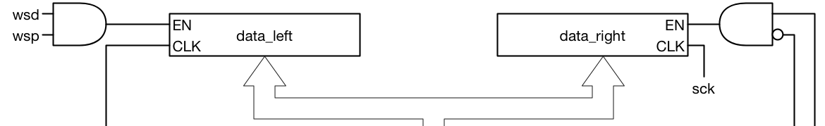
Here is the code for that:
always @(posedge sck)
  if (wsd && wsp)
    data_left <= shift;

always @(posedge sck)
  if (!wsd && wsp)
    data_right <= shift;
Don’t forget the endmodule to close it off.
Thoughts
So there you have it. 296 lines of Verilog code to implement our I2S receiver. Are you happy with it? Probably half of all FPGA designers would pat themselves on the back for a job well done and go on to the next assignment. But really, didn’t you think while typing all those lines of code that it was really repetitive? Didn’t it seem like you should have a computer program to help you type all those lines of code which are almost all the same? Those are signs that we can do a better job.
The Rev B Design
OK, well first we have 33 nets called enn. That is just silly. The first thing we need to do is to make that be a vector. Let’s change the declaration to this.
wire [32:0] en;We also need to change all the places that have enn to en[n]. By my count that gets us down to 264 lines. Still not too much in terms of removing the repetitive nature of things.
The Power of for Loops
Many logic designers don’t understand that you can use Verilog for loops in synthesized RTL code. There is just one simple restriction on their use. The loop you write has to be able to be completely unrolled. What that means is that the loop essentially needs to be run when the code is parsed. It has to take a fixed number of iterations through the loop. The number of iterations has to be known when the code is synthesized.
The Rev C Design
Let’s attack those 33 lines where we make the assignment to the enable bits. First, the enable assignments were continuous assignments to en which was declared as a wire. We first need to change that to a reg so we can assign to it in a combinational always block.
reg [32:0] en;Now, if we don’t use the loop, we would need to code the assignments to EN like this.
always @(*)
  en[0] = count == 0;

always @(*)
  en[1] = count == 1;

...

always @(*)
  en[32] = count == 32;
Even more lines of code! But with a for loop we can code them like this.
integer i;
always @(*)
  for(i=0; i<=32; i=i+1)
    en[i] = counter == i;
That’s it. A big space savings. And it has some other advantages we will discuss later. Let’s attack those assignments to shift while we’re at it.
Bit zero of shift has no reset so it is different. We will leave that alone. But bits 1 through 32 will get written using a for loop.
  always @(posedge sck)
    for (i=1; i<32; i=i+1)
      if (wsp)
	shift[i] <= 0;
      else if (en[i])
	shift[i] <= sd;
Note that we don’t need to declare i again. We are using the same i variable as the previous for loop.
This reduces our design down to 44 lines of Verilog code. That’s a real improvement. But our improvements aren’t over yet.
Parameterization
Notice that the width of our module is hardwired to 32 bits. In the first two designs that is not really an issue because our code was hardwired to 32 bits as well. You couldn’t change the number without adding lines of code to the enable and shift assignments. But with the improvements in version C we now just have numbers scattered around the code which we can derive from a parameter.
In general, I believe you should try to always write your code such that it is parameterized. This more than any other rule will guide you to writing good Verilog code. You should go ahead and change the design to take a parameter called width with a default value of 32.
Remember to use the $clog2 function to determine the number of bits needed for the counter. It might take a little thought to get the expression for the width of the counter exactly right. For a width of 32 the counter should be six bits wide. But if width is 31 the counter should only be five bits. If width is 63 then the counter should still only be six bits.
We will call this version D of the design. But there are more improvements to come.
A Better Encoder
If you run a simulation of the previous design and look at the counter value and the en value you will notice that en is just two raised to the counter. In other words they have the following relationship.
| counter | en | en(binary) |
|---|---|---|
| 0 | 1 | 0000000012 |
| 1 | 2 | 0000000102 |
| 2 | 4 | 0000001002 |
| 3 | 8 | 0000010002 |
| 4 | 16 | 0000100002 |
| 5 | 32 | 0001000002 |
| 6 | 64 | 0010000002 |
| 7 | 128 | 0100000002 |
| 8 | 256 | 1000000002 |
A common way to implement a decoder like this is to just shift 1 left by the count amount. So we can replace our for loop with just the following.
always @(*)
  en = 1<<counter;
Simplifying the shift Assignment
Getting back to the D version of the design, you may recall that we had two always blocks to assign to the shift variable. One used a for loop to assign to bits 1 through 31 because they needed a reset. And a separate one to assign to bit zero where there was no reset. Here is the code for that again.
  reg [0:width-1] shift;
  always @(posedge sck)
    if (en[0]) shift[0] <= sd;

  integer i;
  always @(posedge sck)
    for (i=1; i<width; i=i+1)
      if (wsp)
	shift[i] <= 0;
      else if (en[i])
	shift[i] <= sd;
We can actually merge these two always blocks. If you look at a timing diagram from an existing simulation you will see that wsp is only true then counter is equal to zero. Why? Because wsp actually resets counter. This means when wsp is high, en[0] is also high. If another bit of en is set, then wsp must be low. This means we can remove the else from the second always block. It also means that we can extend the for loop to include index zero now. In the zero case we reset shift[0] in the first if, but we immediately write sd into it with the second if. This has the effect of not resetting it at all. So the new code looks like this.
  reg [0:width-1] shift;
  integer i;
  always @(posedge sck)
    for (i=0; i<width; i=i+1)
      begin
	if (wsp)
	  shift[i] <= 0;
	if (en[i])
	  shift[i] <= sd;
      end
Another Option for the Enable
Instead of shifting 1 left there is another way we can implement the en signal. Let’s change it back into a reg signal and think about the following. As we showed in the last section if you write to the same bit multiple times in an always block it is the last write that actually takes effect. We can make an always block which sets the en value to zero and then just sets the bit indexed by counter to one. That code looks like this.
  always @(*)
    begin
      en = 0;
      en[counter] = 1;
    end
The Biggest Leap
Now let’s out the thinking from the last insight to work for the final thoughts on setting the shift value. First, let’s look at what en is really telling us. Bit n of en is true if counter equals n. So, let’s rewrite the always block where we assign shift to just use the expression for the active bit in en.
  reg [0:width-1] shift;
  integer i;
  always @(posedge sck)
    for (i=0; i<width; i=i+1)
      begin
	if (wsp)
	  shift[i] <= 0;
	if (counter == i)
	  shift[i] <= sd;
      end
Next, let’s factor the reset value for shift to outside the for loop.
  reg [0:width-1] shift;
  integer i;
  always @(posedge sck)
    begin
      if (wsp) shift <= 0;
      for (i=0; i<width; i=i+1)
	if (counter == i)
	  shift[i] <= sd;
    end
Now, if you look at that for loop it should look like one of the dumbest loops ever written. Why is it a loop at all? Let’s fix that once and for all.
  reg [0:width-1] shift;
  always @(posedge sck)
    begin
      if (wsp) shift <= 0;
      shift[counter] <= sd;
    end
Notice that we don’t even need the en signal at all any more.
A Very Subtle Problem
There is a very subtle problem with this design however. It has to do with synthesis. What happens when counter is equal to 32? Well, shift only has bits 0 through 31. So, from an RTL perspective we are assigning to a nonexistent bit. Unfortunately, there is a bug in the Vivado synthesis tool through at least version 2015.1 where this is not what happens. Because of this bug, the counter value is essentially truncated and will set bit zero of shift when counter is 32. You must be extremely careful when indexing into bit vectors and arrays (RAMs) that you don’t exceed the bounds of the vector or array. The synthesis tool will happily wrap those accesses such that they actually modify the vector or array.
You can test this by running the simulation using the synthesized results. You will see that in about half of the cases where the sample size is greater than 32 bits the test will fail.
So we must modify that final always block just a little bit. Here is a fix for the issue.
  reg [0:width-1] shift;
  always @(posedge sck)
    begin
      if (wsp) shift <= 0;
      if (counter < width) shift[counter] <= sd;
    end
This will synthesize correctly since we have explicitly added the check which the synthesis tool should have done automatically.
Synthesis
Speaking of synthesis, I have synthesized each of these designs to see how they compared size wise. Here are the results.
| module | cells | ports | nets | luts | registers |
|---|---|---|---|---|---|
| i2s_receive2a | 218 | 67 | 223 | 42 | 104 |
| i2s_receive2b | 241 | 67 | 246 | 54 | 104 |
| i2s_receive2c | 218 | 67 | 223 | 42 | 104 |
| i2s_receive2d | 218 | 67 | 223 | 42 | 104 |
| i2s_receive2e | 218 | 67 | 223 | 42 | 104 |
| i2s_receive2f | 230 | 67 | 235 | 48 | 104 |
| i2s_receive2g | 230 | 67 | 235 | 48 | 104 |
| i2s_receive2h | 241 | 67 | 246 | 54 | 104 |
| i2s_receive2* | 222 | 67 | 227 | 44 | 104 |
| i2s_receive2 | 230 | 67 | 235 | 48 | 104 |
The design with the asterisk is the final design without the bounds check. The final design is a little larger, but I like the RTL code. It is pretty clean with no for loops and it is quite short. But it is not the smallest in terms of area.
I have linked to each of the designs below.
- i2s_receive2a.v
- i2s_receive2b.v
- i2s_receive2c.v
- i2s_receive2d.v
- i2s_receive2e.v
- i2s_receive2f.v
- i2s_receive2g.v
- i2s_receive2.v
You can follow next part of this tutorial here.