
I2S Transmitter Spec
Let’s take a look at the block diagram for an example transmitter from the I2S spec. It is shown below:
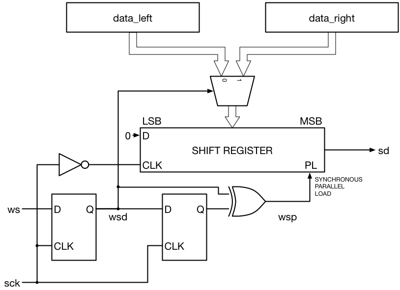
I2S transmitter block diagram
I have also created a timing diagram for the circuit shown in the block diagram. It is shown below:
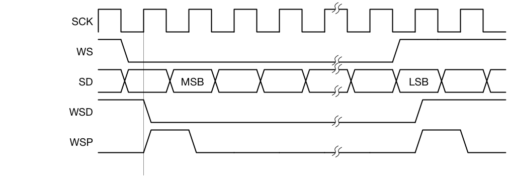
I2S transmitter timing diagram
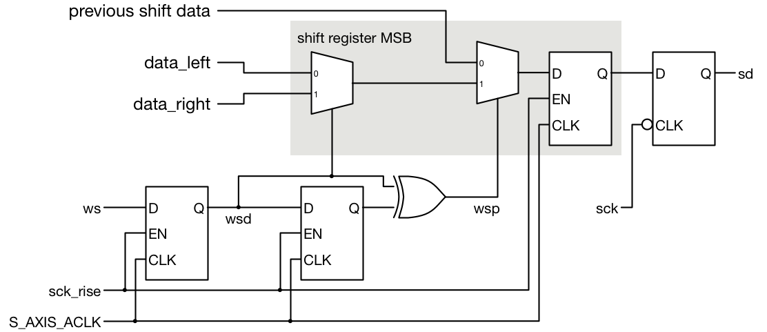
The really important thing to note about the design is the parallel load. The authors of the specification don’t really explain what this means, but based on the requirement that sd change on the falling edge of sck, we can infer they mean what is shown in the detailed block diagram below. In this diagram, I have shown the details of the most significant bit of the shift register. Notice that we have the wsp signal being generated on the rising edge of sck, but it is captured on the falling edge of sck. This makes the circuit dependent on the duty cycle of the sck clock. If it is high for a short period of time we could run into timing issues with the design.
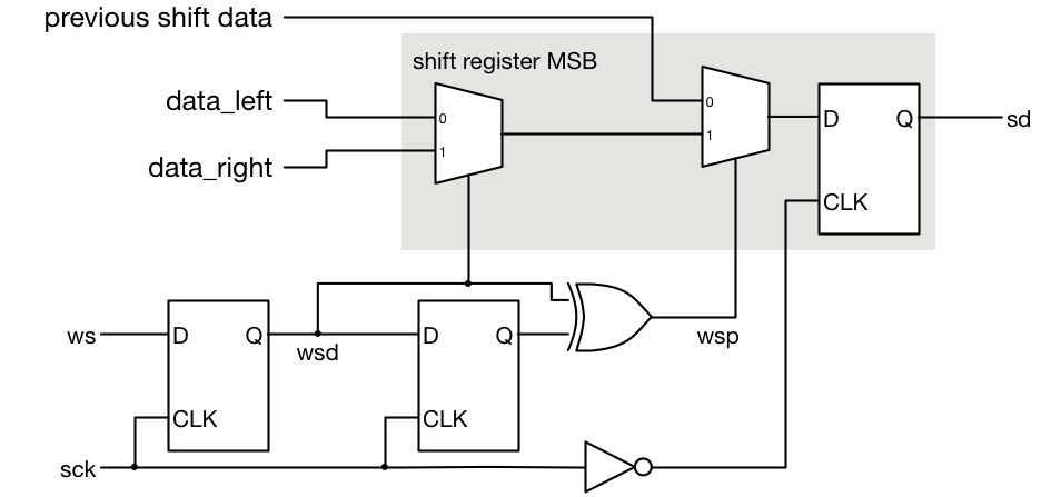
I2S transmitter block diagram details
Changing to the FPGA clock domain
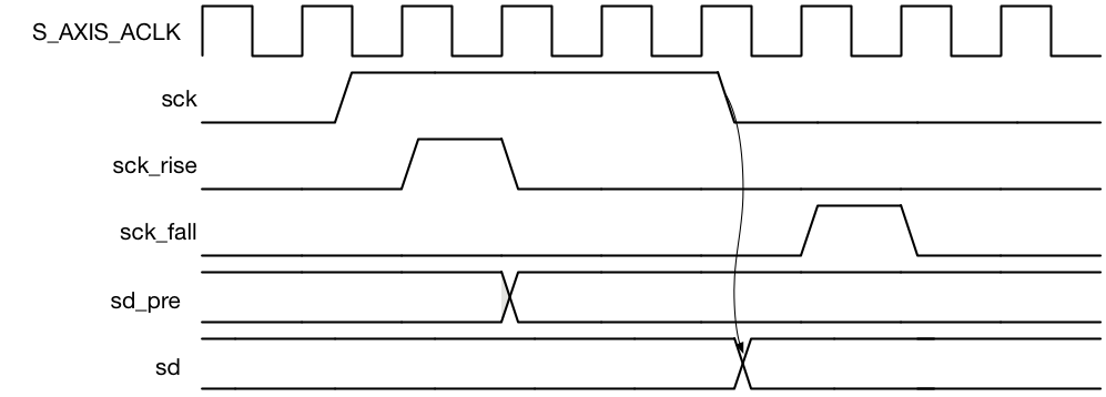
We want to modify the design such that it uses the FPGA clock domain rather than sck. If we just use S_AXIS_ACLK and condition the flip-flops on sck_rise and sck_fall where appropriate, we would get a timing diagram like that shown below:
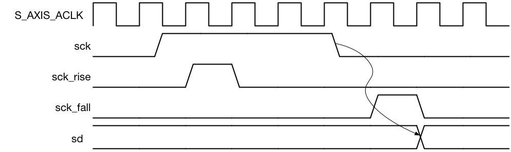
Timing diagram of delay caused by sampling sck
Notice how long it takes from the fall os sck to the change in the output data sd. This can take up to two S_AXIS_ACLK clock cycles. The I2S specification says this is supposed to change when sck falls. We can fix this by shifting the data on the rise of sck but then using a flip-flop clocked off the actual falling edge of sck to generate the data out of the chip. In this situation, it’s not really a big deal to use sck as an actual clock, since it is only going to a single flip-flop. We don’t need to use dedicated clock resources on the FPGA to do this since there is no requirement that skew on the clock tree be balanced. It is balanced by construction because there is only a single clock tree leaf.
The timing diagram below shows the result of doing this. Notice how the sd output is pulled back closer to the falling edge of sck:
Timing diagram detailing reduced delay by clocking sd on the falling edge of sck
A schematic of this is shown below.
Clocking sd out on the falling edge of sck
There are some problems with the design the way it is shown, though. First, we observed previously that the wsp signal was generated on the rising edge of sck, but used on the falling when we load the shift register using the parallel load feature. If we use the logic as it is shown then the wsp pulse will last too long and on the next cycle when we should do a shift we will again do a parallel load. The fix is to not condition the second flip-flop on the sck_rise signal. This will keep wsp as a single clock pulse in the S_AXIS_ACLK domain. This of course means that wsp will not be true while sck_rise is true so we need to remove the enable when the shift register does the parallel load. But of course, we need to keep the enable condition when it comes to shifting the data in the shift register. Our modified design looks something like this:
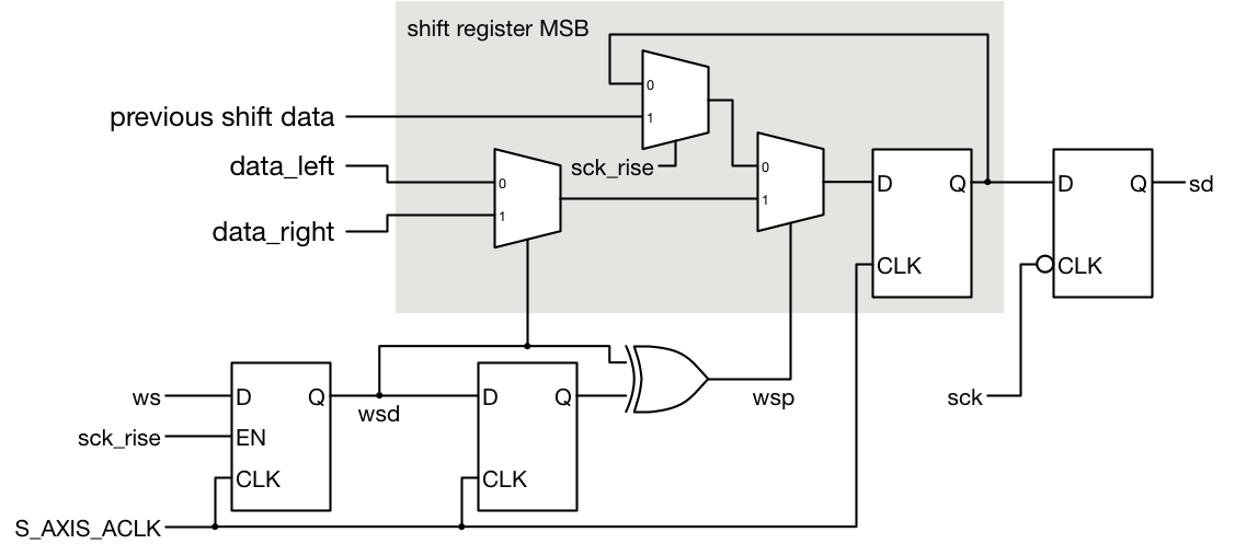
Final I2S transmit block diagram
Test
The test will instantiate your i2s_transmit module and an AXI 4 streaming master module to connect to the slave interface on your design. The basic premise of the test is that it tells the AXI master to write audio data to your transmitter. Your transmitter should take the audio data and write it out the I2S audio interface. The test will drive the audio clock sck and the left/right channel signal ws. Your i2s_transmit module will drive the sd serial data signal. The serial data will be compared against the audio data sent by the AXI streaming master. The figure below illustrates this.
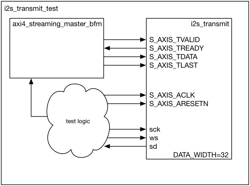
I2S transmitter test block diagram
The ws signal will not be a consistent number of clocks for each sample. The test will vary this period, and your design should accommodate this. Also, your design must keep up with the data driven by the AXI streaming master. While your design determines when it can accept data by asserting the S_AXIS_TREADY signal, it must not wait too long to do so. If your design does not keep up, the test will terminate with an error.
Wrap-up
You still need to design the logic to take data from S_AXIS_TDATA and put it in your data_left and data_right registers. You will also need to design some logic to generate S_AXIS_TREADY to tell the AXI4 Streaming master that you are ready to accept data. I won’t go into detail on that for now so you can have a chance to work it out on your own.
Here are some links to my testbench files:
When running the test (which doesn’t pass) and trying to trouble shoot (the test or my code). . .
I look at the S_AXIS_TDATA under the appropriate valid conditions TVALID=1, TREADY=1, and TLAST and get the following first words
S_AXIS_TDATA
09c0895e left
0db1f056 right
6546df99 left
01893752 right
i2s_transmit_test.check reports:
ERROR: i2s_transmit_test.check: test value 09c0895000, expected 0db1f05000 at time 5750.00ns
ERROR: i2s_transmit_test.check: test value 0d00000000, expected 0900000000 at time 6550.00ns
ERROR: i2s_transmit_test.check: test value 6540000000, expected 0180000000 at time 7550.00ns
ERROR: i2s_transmit_test.check: test value 0189375200, expected 6546df9900 at time 10850.00ns
I presume test value is what my code outputs. I have inspected the serial data output sd for ws and sck and confirmed the first serial data is 28 serial bits in length and is 09c0895 which agrees with the first S_AXIS_TDATA. The “expected” value is looking like the unexpected value to me.
Eric, it looks like the data values are swapped. It is a little confusing though because the test varies the sample size. That is why a lot of the lower bits of the expected values are zero. You can modify the always block which creates the ws signal to always repeat 32 times rather than the random value. This will at least make all the data 32 bits. The sequence of values out from the test is 0x09c0895e, 0x0d81f056, 0x0d00f3e3, 0x3d3823f1, 0xc6c7cfde9, 0xaae2f784. My suspicion is that you have an error where the left and right are getting swapped and there is also a delay of one sample clock for one of the channels. We are getting a little faked out in seeing this though because the first two samples begin with 0x0d and the sample size is really short.
So, try with the change I suggested and see if you can get more information. Also, does every comparison fail? If not it might help to print out all the output values. There can sometimes be clues in what works too.
Send me your i2s_transmit module and I can take a look at it too.
Thanks Pete, good suspicion. I had ws_fall and ws_rise (detect the falling and rising edge of word select) swapped. So appears to pass now. I do get “errors” in that I decided to handle the LSB differently when the I2S request >32 bits provided by the AXI. I choose not to assume zero for LSB but rather wrap the MSB around. The test assumes zero. Thanks, Eric
Pete, is there any chance I could see your i2s_transmit module?
Katie,
Here is a link to the file http://www.beyond-circuits.com/repos/tutorial/trunk/rtl/i2s_transmit.v
Let me know if you have questions.
-Pete
Hi Pete,
Thought you would be interested in that when I was using your original files in the simulation, I got the following output in Vivado:
run all
ERROR: i2s_transmit_test.util.check: test value xxxX000000, expected 0db0000000 at time 8350.00ns
ERROR: i2s_transmit_test.util.check: test value 0db1f04000, expected 3d3b23e000 at time 14450.00ns
ERROR: i2s_transmit_test.util.check: test value 3d3b23c000, expected aae2f78000 at time 19450.00ns
ERROR: i2s_transmit_test.util.check: test value aae0000000, expected ce70000000 at time 22250.00ns
<<>>
Kind,
Zdzislaw
Looks like an issue with the expected values being a cycle early or the DUT values being a cycle late. Which version of Vivado are you using? Nobody has reported this before. I developed the tutorials with 2014.4 so they are pretty out of date at this point.
-Pete
My version of Vivado is 2018.1. The serial data coming out of /shift/ looks good to me, so I figure that it’s the test code that doesn’t register the first right sample. The subsequent samples (both left and right) are registered ok.
It is a race condition in the simulator. Looks like I “fixed” the code to run correctly on Icarus Verilog and ModelSim/QuestaSim. But it doesn’t work on Xsim, which frankly I almost never use. I will see what I can do to get it working on all simulators.
Hi,
In the AXIS interface, I just have valid, ready, id and data lines. I put the condition for reading the S_AXIS_TDATA based S_AXIS_TREADY and S_AXIS_TVALID but I need a solid condition for S_AXIS_TREADY that when it should go high and when to go low. Would you please help me with that? When this module is ready to receive ? when I receive the first ws ?
S_AXIS_TREADY should go high when the unit is ready to receive more data. And it should go low once it has accepted data. That would probably be the cycle after S_AXIS_TREADY and S_AXIS_TVALID are both high.
Hello
can you give me the verilog code of that queue.v