
Verilog
First, we will make the simplest possible FPGA. It will be a wire. Create a new project in Vivado called tutorial1 and add a Verilog file called top.v. You can use the wizard to add ports if you like when Vivado creates the file, or you can add them yourself using the text editor. The design should have a single input called switch and a single output called led.
Edit the file so it looks like this
module top (
  input switch,
  output led
);

  assign led = switch;
endmodule
This declares a Verilog module called top. A module is just a container for part or all of your design. We will learn later that modules can instantiate other modules to create a hierarchical design. But, given that this is the simplest FPGA in the world, that is not necessary.
We declare the module to have a single input called switch and a single output called led. These will correspond to input and output pins on the actual FPGA. The only thing else in the design is the assignment statement. This statement just means that the output led is to change whenever the input switch changes. In effect, it simply creates a wire and connects led to switch.
Constraints
The compiler cannot turn your Verilog code into a working FPGA however because you have not given it enough information. Sure, it knows there is an input pin called switch and an output pin called led, but which pins do you want to use? There are hundreds to choose from. We need to tell it which pins to use. We call this information constraints because it constrains the compiler– it can’t just pick one, but instead must use the one you constrain it to.
Create an XDC constraints source file and call it top.xdc. You should download a copy of the ZedBoard schematics to determine the constraints. But even so, I have included the important information here.
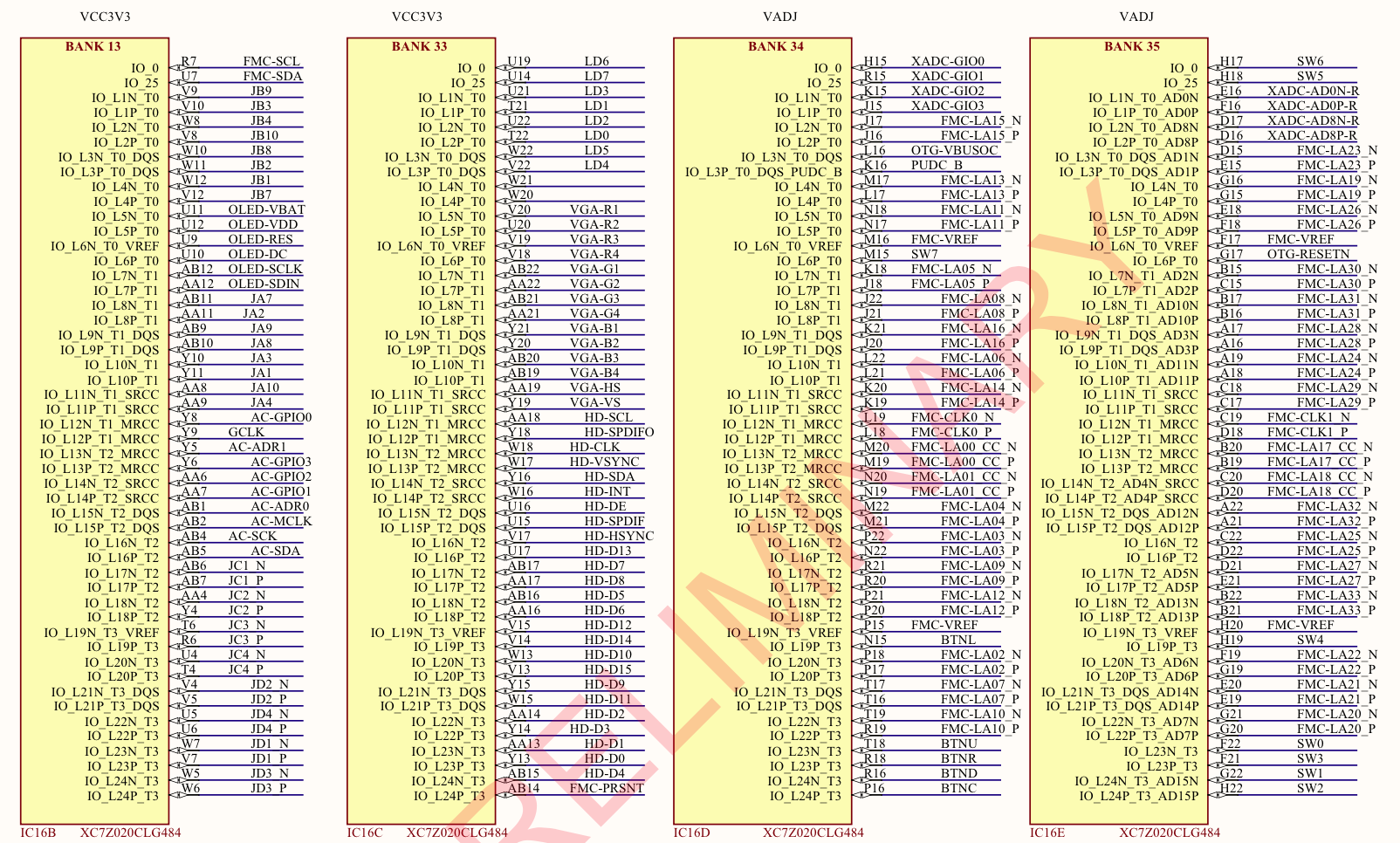
If you look at the schematic, you’ll see that there are eight switches and eight LEDs. Switch 0 comes into the FPGA as SW0 on the schematic and it connects to pin F22 on the FPGA. Notice also that the voltage on the IO bank where the input belongs (bank 35) is VADJ. This voltage is adjustable on the board between 2.5 and 1.8 volts. Assuming your jumper is set to 2.5V, that means this is a 2.5V input.
If you look at the upper left of the schematic you will see a signal called LD0 which is connected to LED 0. This is on a 3.3V bank connected to pin T22. Edit your top.xdc file so that it contains the following constraints. These constraints tell the compiler where we want to connect our inputs and outputs and what logic levels to use for those pins.
set_property IOSTANDARD LVCMOS33 [get_ports led]
set_property IOSTANDARD LVCMOS25 [get_ports switch]
set_property PACKAGE_PIN T22 [get_ports led]
set_property PACKAGE_PIN F22 [get_ports switch]
You should now be able to compile the design. Generate a bit file and program the board. If the blue LED comes on after programming everything should have worked. Slide Switch 0 on and off. The LED should turn on and off as well. Congratulations: you have just created a very expensive and complicated wire!
More Wires
So now let’s modify our design to use a bus of eight wires for the switches and LEDs. since we have eight of those on our board.
Change the Verilog file to
module top (
  input [7:0] switch,
  output [7:0] led
);

  assign led = switch;
endmodule
This will change the inputs and outputs to eight-bit busses. You don’t need to modify the assignment statement. The width of the values just changes from one bit to eight bits. However, the constraints do change a fair amount.
Before, the name of the input pin was switch, and the output pin was called led. Now those values refer to eight pins. We need to apply the PACKAGE_PIN to individual pins. Our constraint files are actually a little program written in the TCL programming language. set_property is a function defined in TCL, and the values passed to it are arguments. get_ports is another function which searches the design database for ports. The square brackets tell TCL to call the function inside them and use the value of the result in place of the brackets. So we can still use the same IO_STANDARD commands. The [get_ports led] call will just return a list of eight ports that match the name led. The set_property command can apply the same IOSTANDARD attribute to all eight. For the PACKAGE_PIN attribute, we need to be more selective. The actual port name for the LSB of the led is led[0]. But we can’t just use this for the name since TCL will try to call a function 0 rather than using the literal characters. We quote the special characters in curly braces. So we will use [get_ports {led[0]}].
Looking at the schematic for all the pin names, we get the following constraints:
set_property IOSTANDARD LVCMOS33 [get_ports led]
set_property IOSTANDARD LVCMOS25 [get_ports switch]
set_property PACKAGE_PIN T22 [get_ports {led[0]}]
set_property PACKAGE_PIN T21 [get_ports {led[1]}]
set_property PACKAGE_PIN U22 [get_ports {led[2]}]
set_property PACKAGE_PIN U21 [get_ports {led[3]}]
set_property PACKAGE_PIN V22 [get_ports {led[4]}]
set_property PACKAGE_PIN W22 [get_ports {led[5]}]
set_property PACKAGE_PIN U19 [get_ports {led[6]}]
set_property PACKAGE_PIN U14 [get_ports {led[7]}]
set_property PACKAGE_PIN F22 [get_ports {switch[0]}]
set_property PACKAGE_PIN G22 [get_ports {switch[1]}]
set_property PACKAGE_PIN H22 [get_ports {switch[2]}]
set_property PACKAGE_PIN F21 [get_ports {switch[3]}]
set_property PACKAGE_PIN H19 [get_ports {switch[4]}]
set_property PACKAGE_PIN H18 [get_ports {switch[5]}]
set_property PACKAGE_PIN H17 [get_ports {switch[6]}]
set_property PACKAGE_PIN M15 [get_ports {switch[7]}]
Make these changes, generate a new bit file, and program the board and now all the switches should control the corresponding LED.
Adding a Clock
One final thing to do is to add a clock. Clocks are important in FPGA designs because they allow the FPGA to have states that vary over time. Make some more changes to your Verilog code. One thing we will be doing is changing the output declaration a little. Notice the reg keyword. In Verilog 2005 there are basically two types of nets: a wire and a reg. Wires are assigned using the assign statement or as outputs of module instances. Reg nets are assigned from inside of procedural blocks. What are procedural blocks, you ask? They are basically blocks of code which behave in a sequential manner. They have some event that activates them and causes them to run. Code within the block runs from start to finish in a sequential manner, just like software.
In the example above, the assign statement said that the output led was equal to the input switch. This isn’t something that is equal only once, and then the system forgets about it. switch and led are always equal. If the right-hand side changes, the left-hand side is updated along with it. This is called a continuous assignment, so named because it happens continuously. As such, it never makes sense to have multiple continuous assignments to a wire. You’ll only ever have one.
We can rewrite the previous code using a sequential assignment like this:
module top (
  input [7:0] switch,
  output reg [7:0] led
);

  always @(switch)
    begin
      led = switch;
    end
endmodule
This tells Verilog to run the code between the begin/end pair every time switch changes. This has the same effect as the continuous assignment. We can also clean up our code a little by removing the begin/end pair since there is only one statement. The part within the@() section is called the sensitivity list. This is a list of variables separated by the keyword or. If any of the variables changes, the always block is reevaluated. We can just use the shorthand notation @(*) as well. This lets the compiler decide which variables have an effect on the outcome and use those instead. So we now have our slightly optimized code, as shown below:
module top (
  input [7:0] switch,
  output reg [7:0] led
);

  always @(*)
    led = switch;
endmodule
We can now add a clock to our design. To do that, we add another input pin called clk and we use that in the sensitivity list for the always block. However, we don’t want any change to clk to sensitize the always block, just the rising edge. So we also use the posedge keyword. Like this:
module top (
  input clk,
  input [7:0] switch,
  output reg [7:0] led
);

  always @(posedge clk)
    led = switch;
endmodule
Now all that is left is to tell the compiler which pin the clock comes in on, its logic level, and finally the fact that it is a clock and it runs at a frequency of 100MHz. So here are the additional lines that we add to the constraints file:
set_property IOSTANDARD LVCMOS33 [get_ports clk]
set_property PACKAGE_PIN Y9 [get_ports clk]
create_clock -period 10 [get_ports clk]
If you compile this, you should see the exact same behavior as before.
Looks like I’m connected OK.
Thanks,
Tim
Thanks for the basic tutorial. really helps. especially there when there are a lot of things to read 🙂
Heya just happened upon your blog from Google after I entered in, “” or perhaps something similar (can’t quite remember exactly). Anyways, I’m pleased I found it simply because your content is exactly what I’m searching for (writing a college paper) and I hope you don’t mind if I gather some information from here and I will of course credit you as the reference. Thank you very much.
tiffanyandcojewelrys.net http://www.tiffanyandcojewelrys.net
Glad to hear it was helpful.
sir/mam,
i am new to fpga, can we assign inputs to pins of a fpga instead of a switch.?
and i also want to know how to buy a fpga for a project? suppose i want to implement a fsk in fpga..which fpga should i buy for my project? fully confused
pls help..thanks in advance
Deepak,
In the tutorials we use input pins of the FPGA that connect to the switches on the ZedBoard. Other pins can connect to other things on the board. It really depends on what the board you are using provides. I can’t really answer your question about FSK because you don’t mention what the input signals and output signals are. Is your design encoding or decoding FSK? Or both? Is it just audio frequency or is it higher? These are all important questions that only you know. It also depends on your budget. The ZedBoard is nice but expensive. The ZYBO board is lower cost but dows not have the FMC connector. I would check the Digilent website as they have a number of low cost FPGA boards and a large number of peripheral boards as well.
Good luck!
-Pete
Really it helps lots to me……………thanx
sir
One things I am not getting here that
You generate clock period using statement “create_clock -period 10 [get_ports clk]”
i am not getting these statement.
Give me few reference to understand this type of clock management.
I am using Zedboard.
I hope for your kind information.
Thanx
Really very helpful for beginners. People tend to get lost in lengthy documentation available on xilinx. Thanks a lot
I am a real beginner,
I have completed this tutorial, but don’t understand meaning of
set_property IOSTANDARD LVCMOS33 [get_ports led]
set_property PACKAGE_PIN T22 [get_ports {led[0]}]
Could someone explain a bit clearly functions/meaning of these above lines?
Many thanks!
Dear Prof. Pete Johnson,
It is so excited when successfully programmed my ZedBoard with your tutorial!
please recommend a Verilog book so that I can practice more!!
Thank you,
I don’t have any good Verily book recommendations. I mostly use the standard document from IEEE.
The IOSTANDARD property tells the tool that you are using a 3.3V CMOS IO. The PACKAGE_PIN property tells the tools which pin of the chip you want to have the led[0] signal connected to.
I am glad it was helpful.
Hi sir,
How is this differ from creating block design?
How do i program the fpga? Is it through sdk?
I’m very new to fpga and I use zedboard.
Thank you in advance 🙂
Block designs and when you would use them are covered in later tutorials. This first tutorial is just designed to let you make something happen. To program the FPGA, you just go to the Hardware Manager and Open Target. Vivado walks you through what you need to do. You need to have your board connected to the machine you are running Vivado on.
Great tutorial for any beginners. Thanks a lot…
My synthesis keeps failing with the complaint on “led = switch” that procedural assignments to a non register led is not permitted.
Changed the declaration of led from
output [7:0] led
to
output reg [7:0] led
and the synthesis compiled without error.
does this work?
Thanks in advance
Yes, that changes the type from wire to reg and allows the procedural assignment.
Hi Pete,
I am very new to this FPGA stuff.
Do you know of any resources that may help a beginner?
Thanks
Jeffrey
Well, my tutorial is pretty geared towards beginners. To follow it exactly you need a ZedBoard which is fairly expensive – although not by FPGA board standards. You could also adapt most of the tutorial to the ZYBO board which is much less expensive. Also, Digilent offers significant student discounts if you are a student.
Hey Pete thanks for your tutorial,
I have a bitstream error ‘logical ports have no user assigned specific location constraint (LOC).’
I know what it means, but my PACKAGE_PIN and IOSTANDARD is defined for this pin.
Any idea how to fix it ?
It’s probably a typo in your constraints. Or you have an extra port that you forgot to specify a location for. Can you post your code and constraints? Or you can email them to me and I’ll take a look.
thank you. I don’t think it’s a typo, what is your mail ? Mine is nathan.cavaglione@gmail.com
I will send you the constraints and small Verilog code. Still have not spotted what is wrong
My email is pete@beyond-circuits.com.
I sent you a mail
I haven’t received your email yet. You might want to double check the address and that it was sent.
This is great stuff…many thanks for making the effort to put it together
Congratulations on such great tutorial!
I was trying to play with this first example. What if I want to light up the LEDs randomly?
I tried to assign
led = $random
inside the always block but it didn`t work.
All LEDs were off and no error message was given. My guess is that the clock is too fast for the LEDs to, actually, turn on or off in time to see some difference. Any thoughts on how to do that?
Thanks again for the attention
That is a good question. One thing that you need to get a good feel for is what things are verification constructs and what are logic constructs. A lot of Verilog works in the simulator for testing your design but doesn’t express actual hardware constructs. Only a subset of Verilog is actually supported for hardware synthesis inside the FPGA. In this case, $random is only a verification construct. It has no meaning when you ask the synthesis tool to make gates.
What you really need is some type of logic that can make a pseudorandom bit. Of course you can’t design a piece of logic which makes a truly random value. One simple structure that makes a pseudorandom bit is called a linear feedback shift register. They are actually pretty easy to construct in Verilog. You can download my version here lfsr.v. You will also need to use a clock and reset signal. You will also probably want to add an enable signal so that you can slow down the update of the LFSR. Otherwise it will change too fast to be visible. Do a couple more of the tutorials to get a feel for some of these things. You should be able to learn enough to do what you want after a few tutorials. And feel free to ask if you need tips or suggestions.
Thanks for the reply. My ultimate goal is to learn how to interface a daughter card that I have with the FMC-LPC of the ZedBoard. This tutorial has been one of the most helpful from a few that I have been through.
If you have any material or example for the FMC, that would be great!!
I don’t have any tutorials specifically with the FMC connector. But it’s pretty simple. You just use the ZedBoard schematic to follow the FMC pin back to the FPGA pin. Then you use the schematic of the daughter card you are using to follow from the FMC connector on the daughter card to whatever it is you want to control on the daughter card. What is the daughter card you are trying to use?
It is a FMC 150. It is an integrated ADC and DAC converters. The idea is to create sinusoidal electrical signals to send to a MUT and read back. Comparing these two signals, we will be able to determine characteristics of the materials we are working.
I do not have the PmodSSD circuit for the next Tutorials but probably will do the simulations for it. I`m guessing that FMC150 will be similar to interface but with more pins in the constraint files.
http://www.4dsp.com/FMC150.php
Yes, it’s just a matter of figuring what pins do on the ICs on the FMC card and then tracing those back through the FMC connector and on to the ZedBoard. Then follow them through to the FPGA. Then set the pin constraints so that the pins of the FPGA internals match up. Do you have a good feel for the logic that you will be putting inside the FPGA? You probably need a DDS and some filtering on the signal coming back in from the ADC.
About the logic, not really. I have a professor helping me out on this project so I will probably ask for his advice when I feel comfortable about HDL and the ZedBoard.
It is a matter of studying the daughter card deeply also. It has quite a lot of pins and I am not sure what is the function of each one of them. The datasheet is not that clear, that`s why I was looking for an example project. I still have to take a look at the ones in ZedBoard.org but the approach is different. It is more about using the HDMI connection and cameras attached to it. Thanks for the interest though, I am pretty sure I`ll be more comfortable after completing the tutorial
Good luck with your project. Feel free to contact me if you have questions or want to bounce ideas off someone.
I am new in FPGA .
How can i compile this code and run it in zedboad ?
thanks for your great tutorial.
You need to download the Xilinx Vivado tools and install them on your computer. After that you need to run them and create a new project. You can set the board type to the ZedBoard when you create the project. Then follow along with the tutorials. The tutorials will not guide you explicitly through every step. You will need to read and understand the tutorials and work some things out for yourself. Feel free to ask if you get stuck.
-Pete
Thanks sir.
Do you know if I can use PYNQ-Z1 with your tutorial? I ask because PYNQ is sold for only $65 at digilent. Thanks.
You can do many of the tutorials with the PYNQ. You can’t do the ones involving audio though. They use a chip which is specific to the ZedBoard. You will need to use different pin constraints though. The tutorial walks you through how you figure these out, so you should be able to do it. Let me know how it works out for you.
Do you have to do anything special to get the FPGA (PL) only tutorials working? I have read that the processor (PS) must be running to support FPGA but you seem to be using just Verilog and Vivado and generating your bitfile. I do not know whether this is true but I would like to know if I can develop/learn FPGA in isolation on something like a Pynq or Arty Z7. Really enjoyed reading tutorials looking forward to trying them out if this is possible on these boards.
do you know xdc for slice implementation??
How do you access the 16 auxiliary channels of XADC in Zedboard ? Can I use the existing I/O pins as auxiliary inputs ? I couldn’t find any options to change the sites of auxiliary channels. Should I use an FMC breakout board to access all analog channels ?
You don’t need the PL to do anything. Simply ignore it and the FPGA will function file with just the PL.
I am currently trying to generate a clock signal of 1MHz using the inbuilt clock of 100MHz. I want to get the clock output from PMOD JA connector pin, but am unable to get that. I tried a simple toggle of a port at every positive edge of the clock and I set the constraints file for the clock as specified by you in Tutorial 1 of beyond circuits.
Also, when I try to use the clock pin of Y9 in my constraints file, I get a warning that states: “Debug Hub Core was not detected at User Scan Chain 1 or 3”. Can you help me out with this too?
Your help and support will be appreciated.
So Y9 is the 100MHz clock input. In tutorial 3 I have the following constraints for that input which I call clk.
set_property IOSTANDARD LVCMOS33 [get_ports clk]
set_property PACKAGE_PIN Y9 [get_ports clk]
create_clock -period 10 [get_ports clk]
Let’s assume you want your 1MHz clock to go out JA1. That is on Y11. And I will call it clkout.
set_property IOSTANDARD LVCMOS33 [get ports clkout]
set_property PACKAGE_PIN Y11 [get_ports clkout]
Now in the Verilog you need to declare the ports and make a counter. The counter will count from 0 to 99 and then wrap. You will also use a flip-flop to capture the output clock value. Here’s some possible code
module clk_gen(input clk, output reg clkout);
reg [7:0] cnt = 0;
always @(posedge clk) if (cnt == 99) cnt <= 0; else cnt <= cnt+1; always @(posedge clk) if (cnt == 49) clkout <= 1; else if (cnt == 99) clkout <= 0; endmodule This should give you a 1 MHz output clock. Your warning indicates that the clock that is going to an embedded logic analyzer is not running. This could be because you didn't specify the right location for the clock input. Or because you didn't connect a functioning clock to the logic analyzer. My guess is that this warning will go away once you get things hooked up correctly. Let me know if you have more questions. -Pete
Hi Pete,
The code worked. Thank you for your help.
Oh my gosh thank you so much for these tutorials! I came here looking for help learning how to use AXI interfaces but I’m going to systematically go through most of the FPGA tutorials here. About the AXI situation: I had been watching youtubes to learn but for AXI there seemed to be no skilled teachers, only reference guides and people who “teach” like they’re reading a ref guide to you. Verbatim. I had too many professors like that. Thanks again and I’ll be getting to that AXI stuff (like in Tutorial 18) soon! 🙂 Oh by the way I use an Arty board, with Vivado, which I love.