
In this tutorial, we will develop an I2S audio receiver. The goal of the tutorial is to really give you a chance to write your own RTL code. The tutorial will give you a simulation test bench which you will use to verify your RTL code. The tutorial will proceed in a number of steps, with each step adding more to your design. Let’s get started.
I2S Overview
The I2S protocol is a common standard used to send audio data. It is a serial protocol very similar to SPI, but it is a streaming protocol. That means it is always transmitting data.
I2S sends a stream of stereo audio data. For each audio sample there is a left channel and a right channel value. The values can be any number of bits, although 16, 20, 24, and 32 bit values are the most common. The I2S Bus Specification provides a really good overview of the protocol and you should download and peruse that link now.
There are three signals involved in sending audio data. A serial clock SCK, a word strobe signal WS which indicates if the data is for the left channel or the right channel, and a serial data signal SD. The WS and SD signals are synchronous to the SCK signal and change on the falling edge of SCK. Data is sent most significant bit first. One wrinkle is that the data is one cycle late with respect to the word strobe. The timing diagram illustrates the details.
Implementing the Receiver

I2S protocol timing diagram
In the next few tutorials, we will be using a technique called Test Driven Development. With Test Driven Development, you write the test first and then write the RTL code that passes the test. Then you add more to the test, then add more to the RTL to again pass the test. By iterating this way, you get to the point where the test tests everything you want and the RTL performs the correct function. I will be providing the test code and it is your job to write the RTL. I will also give you a block diagram for the RTL so you have a good idea of what you will need to code.
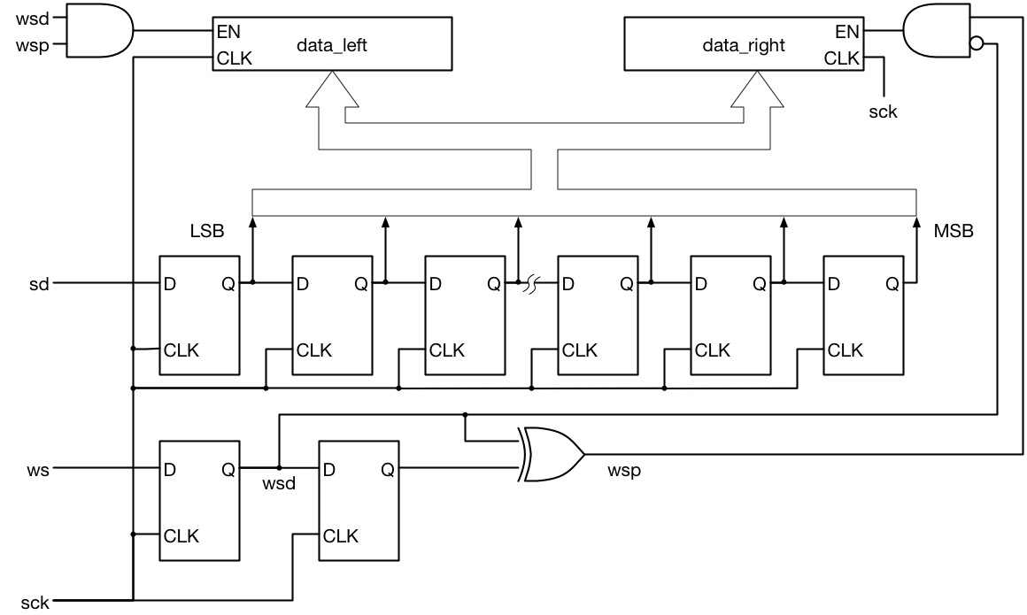
Basic I2S receiver block diagram
For our first pass, we will implement a receiver that has a fixed 32-bit word size. The block diagram (almost schematic) is shown to the right. This figure is largely taken from figure 6 of the I2S specification. However, I believe the figure in the specification is actually incorrect. The specification has the polarities of the WSD signals into the AND gates, which enable data from the shift register to be written to the left and right data registers.
Ideas and Tips
Here are some ideas and tips about designing this module.
First, remember that an HDL like Verilog describes the hardware. You are not describing a task or a sequence of steps like you would in software. You need to take the block diagram and code each piece of it.
Registers with enables
So for example, data_left and data_right are 32-bit output registers which are clocked off of sclk and they each have an enable. How do you code a register with an enable? Here is an example.
always @(posedge clk)
  if (enable)
    my_reg <= my_value;
The enable expression can be more complex than a simple value. But, the result of that expression will enable the register my_reg to update its value.
Combinational Logic
How about the output of a combinational gate? Let’s say we have values a and b and we want to create the signal z which is the logical OR of a and b? Well, there are two ways that we can do this in behavioral Verilog code. We can declare z to be a wire and use a continuous assignment like this:
wire z;
assign z = a|b;
We can even combine the wire declaration and the assign statement into a single line like this:
wire z = a|b; We could also use a combinational procedural block and a reg variable like this:
reg z;
always @(*)
  z = a|b;
Note a couple of things. First, we need to use a blocking assignment and not a non-blocking assignment. If we were to use a non-blocking assignment, weird interactions with the combinational always block and other sequential blocks could cause incorrect simulation results. Basically, if you were to use a non-blocking assignment and then assign the z value into a flip-flop, whether you get the updated value of z would depend on simulation ordering of the events. It would lead to the simulation being incorrect and not matching the synthesized design.
Second, it is critical that all paths of execution in the always block assign a new value to z. If this is not the case, then you are specifying that there may be conditions where z does not update and should hold its value. This implies a latch type construct. The only time you should need to use a latch is interfacing with some unusual external logic. I have designed dozens of FPGAs and have only needed a latch once or twice.
Shift Registers
There are a number of ways to code a shift register. Say we have a four-bit register called shift that shifts a value shift_in in the least significant bit.
You could code this the C way:
reg [3:0] shift;
always @(posedge clk)
  shift <= (shift<<1)|shift_in;
You could code this the VHDL way:
integer i;
reg [3:0] shift;
always @(posedge clk)
  begin
    shift[0] <= shift_in;
    for (i=1; i<4;i=i+1)
      shift[i] <= shift[i-1];
  end
You could code this the caveman way:
reg [3:0] shift;
  always @(posedge clk)
    begin
      shift[0] <= shift_in;
      shift[1] <= shift[0];
      shift[2] <= shift[1];
      shift[3] <= shift[2];
     end
Or the more literate Verilog way:
reg [3:0] shift;
always @(posedge clk)
  begin
    shift[0] <= shift_in;
    shift[3:1] <= shift[2:0];
  end
Or the more aesthetic Verilog way:
reg [3:0] shift;
always @(posedge clk)
  shift <= {shift,shift_in};
Some people, and more importantly, some linting tools will complain about the above code. The complaint is that the expression on the right is five bits and the value on the left is four bits and so we are dropping a bit. My rebuttal to this is “Well, of course we are. We don’t need that bit any more.” They would have you write the code like this:
reg [3:0] shift;
always @(posedge clk)
  shift <= {shift[2:0],shift_in};
I guess that is well and good, but with this new code, in addition to being more verbose, you need to modify two lines of code if the width of the shift register changes. In general, I don’t think it looks as clean and prefer to just turn off those warnings with the lint tool.
Anyway, hopefully these tips will help you to code the module.
Files
Here are the files you will need. The test file uses another module called common_test_util for some housekeeping tasks. You will need to have both of these files in your simulation as well as your RTL file.
Your Verilog RTL file should be called i2s_receive1.v and contain a module called i2s_receive1. This module should have input ports called sck, ws, and sd, as well as two 32-bit output ports called data_left and data_right.
Next Steps
You can go to the next tutorial where we improve the I2S receiver here.
Hi Pete,
Why do you use .sv as a test file extesion? Should it be .v?
Susan
Susan,
.v is used for Verilog and .sv is used for SystemVerilog. When I originally wrote the test I used SystemVerilog queues. But the Vivado simulator does not support those. I just didn’t change the extension back to .v. The files are now plain Verilog so you can change it. Or leave it .sv. It doesn’t really matter.
-Pete
Hi Pete,
I have the following doubts can you please help me with this.
1) Are digital values obtained from adau1761_adc_sdata pin actual audio data?
2) If I want to capture the audio data for a few seconds and store them . Should we use I2S protocol to capture this or can we directly store them in a register.
Can you suggest me on the clock value to be used to do this?
Jeepali,
Yes, the data from the ADAU1761 is the actual audio data. Look at tutorial 21 to see how to store the data in a RAM. If you want to store the audio data for a few seconds then it would be best to have the ARM store the data in its memory. It would be pretty easy to use a DMA controller to take the AXI4 streaming data from the I2S receive module designed in tutorial 18. You could also use a DMA controller to stream the data from memory back to the I2S transmitter discussed in tutorial 19. If you work through all the tutorials you should have all the tools you need to store and play back audio.
Hi Pete ,
Can you please help me understand how the sampling of data happens in ADAU1761?
The output(adau1761_adc_sdata ) that we are getting is a stream of bits at the rate of bclk , and the values are stored in 32 bit registers, does this mean the sampling rate of the audio signal is (bclk/32) ?
Will I be right to read each of these samples as signed numbers to get each sample value ?
Thanks in advance,
David.
David,
The way the I2S receiver works is to align the most significant bit of the sample with the most significant bit on the 32-bit bus. But there is nothing that says that the adau1761 sends 32 bits per sample. In fact it doesn’t. I don’t recall what the number is, but I think it is either 20 or 24. The way the interface works though it really doesn’t matter. The adau1761 could send 64 bits of data for each channel and things would still work. Our receiver would just drop the low order 32 bits.
So, you can just treat the data as a signed 32-bit value and everything should work fine. To know exactly how many bits per sample the adau1761 is sending you can turn on debugging on the I2S interface and watch the data. That would tell you.
I hope this helps.
-Pete
Hi Peter,
I see data_right and data_left enables which wsd is using is in wrong notation in receiver figure .
This enables must be exchanged because according to specification of I2S bus
The word select line indicates the channel being transmitted:
• WS = 0; channel 1 (left);
• WS = 1; channel 2 (right).
Thanks & Regards
Vishal Vishwanath
It seemed to me when I did this that the figure in the standard was wrong. In the code that I implemented I verified that the left and right channels were correct. Maybe I need to review this again.
Hi Pete,
I found that the shift registers used in the receiver are supposed to be triggered by the positive edge of the sck, otherwise, it would introduce one additional clock delay in the signals of data_left and data right. I am not sure why it does happen.
I thought
always @(negedge sck)
a<=b;
c<=d;
these two assignments are suppposed to being set at almost the same time. It would not introduce any delay.
Could you please give me some hints on this?
Regards
Alex
Pingback: FPGA music visualiser – part 2 – Cam Beaney's Blog
Hi Pete,
This tutorial is great, I try to follow each step to get familiar with Xilinx tools. But now seems the link for common_test_util.v is private, would you mind make public downloadable?
Regards,
Jun
Hi Pete, sadly, the access to common repo is not available. Would it be possible to fix the link to the common file?
Hi Pete, I’m trying to work on the I2S receiver with given sample. However it seems I don’t have access to the common_test_util.v file. Could you please help with it? Thanks!
Hi, thanks for the tutorial. I am trying to download common_test_util.v but it is asking for a username and password
Should be fixed now.