
Overview
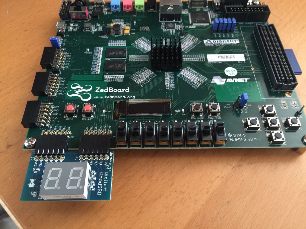
In this tutorial, we will use the switch inputs to drive a seven segment display. The display is the PmodSSD from Digilent. You will need to connect the PmodSSD to the ZedBoard as shown in the photo below if you want to use the same pin constraints that I use in this tutorial.
The First Digit
Ports
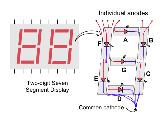
The two-digit display uses seven pins to control the seven segments of each display and one pin to select which display to drive. To display using both digits, you need to alternate between the two digits faster than the eye can perceive. This makes it look like both digits are displayed at the same time. For our purposes, we’ll start by displaying just one digit. We will need to add some new output pins to our design: a seven bit bus called ssd, and a single bit output to control the digit select. This line connects the cathode of the display, so we will call it ssdcat. The module declaration should look like this.
`timescale 1ns/1ns
module top (
  input clk,
  input [7:0] switch,
  output reg [7:0] led,
  output reg [6:0] ssd,
  output reg ssdcat
);
LED Mapping
Each digit has seven LEDs, labeled A through G, shown in the figure below:
To make the digits, we activate the LED values according to the figure below:
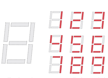
We will add a pattern for 0 as well, and we also can add patterns for the hex digits A, b, C, d, E and F. Note that we can’t make uppercase versions of B and D because they would appear the same as the numbers 8 and 0. For the output value, I am connecting the most significant bit to LED A, and the least significant bit to LED G. The Verilog notation for binary numbers is to use a width value, followed by an apostrophe (tick), followed by the letter “b”, followed by the binary digits.
| Input Valut | Segments Lit | Output Value |
|---|---|---|
| 0 | A B C D E F | 7'b1111110 |
| 1 | B C | 7'b0110000 |
| 2 | A B D E G | 7'b1101101 |
| 3 | A B C D G | 7'b1111001 |
| 4 | B C F G | 7'b0110011 |
| 5 | A C D F G | 7'b1011011 |
| 6 | A C D E F G | 7'b1011111 |
| 7 | A B C | 7'b1110000 |
| 8 | A B C D E F G | 7'b1111111 |
| 9 | A B C F G | 7'b1110011 |
| A | A B C E F G | 7'b1110111 |
| b | C D E F G | 7'b0011111 |
| C | A D E F | 7'b1001110 |
| d | B C D E G | 7'b0111101 |
| E | A D E F G | 7'b1001111 |
| F | A E F G | 7'b1000111 |
We will use the four low bits of the switch input to drive the LED digit, as well as the Verilog case construct to implement our table. Your code should look something like this:
  always @(posedge clk)
    case (switch[3:0])
      0: ssd <= 7'b1111110;
      1: ssd <= 7'b0110000;
      2: ssd <= 7'b1101101;
      3: ssd <= 7'b1111001;
      4: ssd <= 7'b0110011;
      5: ssd <= 7'b1011011;
      6: ssd <= 7'b1011111;
      7: ssd <= 7'b1110000;
      8: ssd <= 7'b1111111;
      9: ssd <= 7'b1110011;
      10: ssd <= 7'b1110111;
      11: ssd <= 7'b0011111;
      12: ssd <= 7'b1001110;
      13: ssd <= 7'b0111101;
      14: ssd <= 7'b1001111;
      15: ssd <= 7'b1000111;
    endcase
We also need to drive the ssdcat output as well. For now, let’s just set it to zero.
always @(*) ssdcat = 0;Of course, let’s not forget to end our module with the endmodule keyword.
Constraints
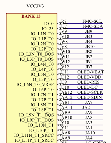 Since we have declared new outputs, we need to add some new constraints. If we look at the schematic for the ZedBoard, we see that the JA1 and JB1 connectors that we’ve plugged our PmodSSD into are connected into the 3.3V bank 13. So, we’ll have to constrain those pins as 3.3V IO.
set_property IOSTANDARD LVCMOS33 [get_ports ssd]
set_property IOSTANDARD LVCMOS33 [get_ports ssdcat]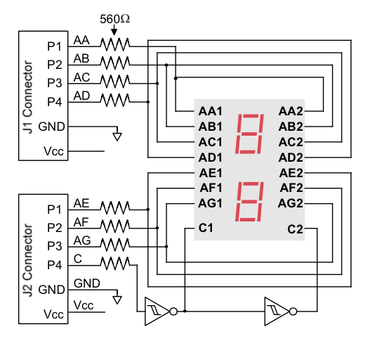 We also need to figure out the pin assignments. To do this, we need both the schematic for the ZedBoard, as well as the pinout for the PmodSSD. If you look on the ZedBoard where the PmodSSD connects, you can see which pins on the JA and JB connectors correspond with which pins on the PmodSSD. Pins JA1, JA2, JA3, and JA4 match with pins AA, AB, AC, and AD, respectively, while pins JB1, JB2, JB3, and JB4 match with pins AE, AF, AG, and CAT. Following all the connections leaves us with the following constraints:
set_property PACKAGE_PIN Y11 [get_ports {ssd[6]}]
set_property PACKAGE_PIN AA11 [get_ports {ssd[5]}]
set_property PACKAGE_PIN Y10 [get_ports {ssd[4]}]
set_property PACKAGE_PIN AA9 [get_ports {ssd[3]}]
set_property PACKAGE_PIN W12 [get_ports {ssd[2]}]
set_property PACKAGE_PIN W11 [get_ports {ssd[1]}]
set_property PACKAGE_PIN V10 [get_ports {ssd[0]}]
set_property PACKAGE_PIN W8 [get_ports ssdcat]
Hello,
Thank you for super great tutorials,
I have done simulation for this tutorial since my seven led display is still on ordering… I have two questions.
1) “always @(*) ssdcat = 0;” can we predict which digit/ (seven led) is chosen or turn on?
2) What happen if we change the clock from 100MHz to 100Hz?
Thank you!!!
When ssdcat is low I think the left digit is turned on.
Dear Sir Pete Jonhson,
Nothing important, I just excited…
My seg led arrived today, and I saw the RIGHT digit on. (I place the board, connect digits same as your picture in this tutorial).
Pingback: Lab 4: Let get the seg-led on – tranminhhai
Congratulations. I’m glad to hear that things are working well for you. Let me know if you have more questions.
Pingback: Adding Functionality to a Project
Hi Pete,
Thank you for your tutorials. I know Verilog from my undergrad but w/ your tutorials I am really learning how to apply those concepts and do real-world digital design on Zedboard. Keep it up. Look forward to your next tutorials!
Frank
Hi Pete,
Could you write a tutorial or explain how to constrain the pins on the SDP breakout board provided by Analog Devices? These are the specs: http://www.analog.com/media/en/technical-documentation/user-guides/UG-282.pdf
I am trying to understand how to use this breakout board to pilot my own external devices but still haven’t figured out how to assign my pins to the actual breakout board pins. So if I try
set_property PACKAGE_PIN J1-43 [get_ports {led[0]}] # page 11 of the specs, GPIO0
The bitstream generation fails. Could you suggest me how to do this?
Thanks,
Frank
Frank, I’m glad you’re enjoying the tutorials. I will try to add more but things are pretty busy right now.
-Pete
When you specify the package pin in the XDC file you are describing the pin on the FPGA which is to connected to the internal signal in the RTL. J1-43 is a reference to your specific board. Vivado has no way of knowing anything about this board. You have to look on the schematics on whichever board is connecting to the AD board and follow the signal back through whatever connectors connect it to the FPGA board. From there you need to follow the signals back in to the FPGA and determine which FPGA package pin the signal goes to.
You may have been a little confused because Vivado can be taught about specific boards like the ZedBoard. But it doesn’t know about your board or how it is connected to your FPGA board so you will need to do the legwork to trace things out.
I hope this helps. Let me know if you have more questions.
-Pete
Test Bench file for the tutorial 4
`timescale 1ns / 1ns
module bench;
reg [7:0] switch;
wire [7:0] led;
reg clk=1;
reg [7:0] expected_led;
wire [6:0] ssd;
reg [6:0] expected_ssd;
always #5 clk = ~clk;
top UUT (.switch(switch), .led(led), .clk(clk), .ssd(ssd));
always @(posedge clk)
switch = $random;
always @(posedge clk)
expected_led <= switch;
always @(*)
case (switch[3:0])
0: expected_ssd = 7'b1111110;
1: expected_ssd = 7'b0110000;
2: expected_ssd = 7'b1101101;
3: expected_ssd = 7'b1111001;
4: expected_ssd = 7'b0110011;
5: expected_ssd = 7'b1011011;
6: expected_ssd = 7'b1011111;
7: expected_ssd = 7'b1110000;
8: expected_ssd = 7'b1111111;
9: expected_ssd = 7'b1111011;
10: expected_ssd = 7'b1110111; //A
11: expected_ssd = 7'b0011111; //b
12: expected_ssd = 7'b1001110; //C
13: expected_ssd = 7'b0111101; //d
14: expected_ssd = 7'b1001111; //E
15: expected_ssd = 7'b1000111; //F
endcase
integer num_checks = 0;
integer num_errors = 0;
always @(posedge clk)
begin
num_checks = num_checks+1;
if (expected_led != led)
begin
$display("ERROR: led value %x does not match expected value %0x at ", led,expected_led,$realtime);
num_errors = num_errors+1;
end
end
integer num_checks_ssd = 0;
integer num_errors_ssd = 0;
always @(posedge clk)
begin
num_checks_ssd = num_checks_ssd+1;
if (expected_ssd != ssd)
begin
$display("ERROR: ssd value %x does not match expected value %0x at ", ssd,expected_ssd,$realtime);
num_errors_ssd = num_errors_ssd+1;
end
end
initial
begin
repeat (1000) @(posedge clk);
$stop;
end
Could you make a tutorial for the onboard OLED display? Thank you so much!
The ZedBoard is starting to get pretty old. I don’t think I will be doing any more tutorials with that board.
Why do we use switches here? And why do we define 4 (3: 0) switches in the case?
The tutorial is just using the low four bits of the eight switches to give us a 4-bit value to drive a hex digit. The next tutorial will expand on these ideas.