
In this tutorial, we will use the stopwatch IP block that we build in tutorial 12 to build an FPGA which includes the ARM processor.
Getting Started
Open the stopwatch_controller project you built in tutorial 13. If you have just completed tutorial 13, Vivado should already be open to the correct project. If not, just open the project in Vivado or follow the initial directions in tutorial 13 to create the project.
Adding the repository
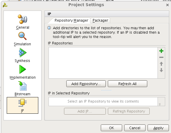
If you are creating a new project, you may need to add the IP repository that holds the stopwatch_controller that we designed in tutorial 13. To do that, select Project Settings from the Project Manager flow. This will bring up the Project Settings dialog box. Click the IP tab and then click the Add Repository button. Navigate to the ip_repo directory you created in tutorial 13 and add the repository. 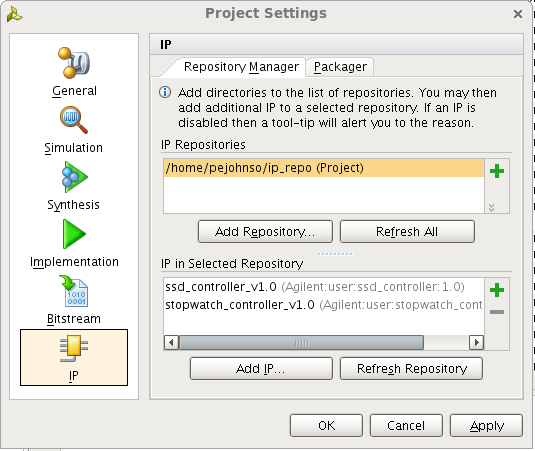
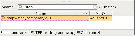
You should see the stopwatch_controller listed as an element in the repository similar to the figure to the right. Go ahead and click OK to dismiss the dialog box.
Creating the block design

Click the Create Block Design link in the IP Integrator section of the Flow window.
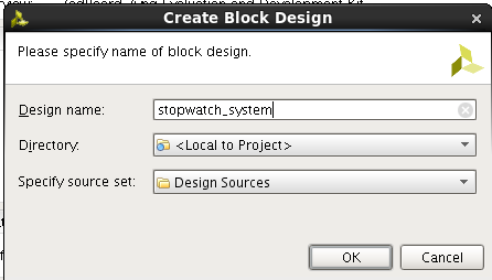
This will bring up the Create Block Design dialog box. Enter the name stopwatch_system and click OK.
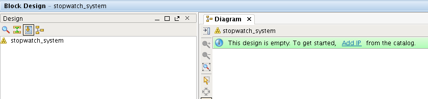
 This will bring up a Block Design window. You will see a sub-window called Diagram with a prompt to Add IP from the catalog. Go ahead and click the link. This dialog box will show you all the available IP. The easiest thing to do is to start typing the first few letters of the IP block you want to instantiate and then press enter to instantiate the block. You will then see a block diagram component representing our stopwatch_controller IP block.
 Next, click the Add IP button to bring up the IP dialog box again. This time we will select the ZYNQ ARM processor. Go ahead and type ZYNQ into the search field. You will see two different ZYNQ IP blocks. One is a bus fu
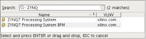 nctional model (BFM) for simulating the ZYNQ design. The other is the ZYNQ processor itself. Select the ZYNQ processing system and press Enter.
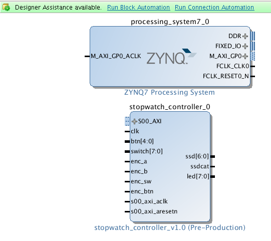 You should see two instances in your Diagram window now: one for the ARM and one for the stopwatch controller. There are also two Designer Assistance links. The Run Connection Automation link will connect the ZYNQ ARM processor to the stopwatch controller. Go ahead and click that now. This will bring up a dialog box. Just go ahead and click OK. Notice that a few more IP blocks, a reset controller and an AXI interconnect block.
Next, go ahead and click the Run Block Automation link. Click 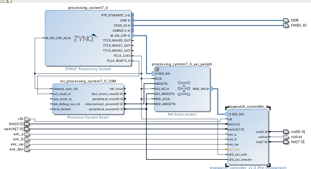 OK to dismiss the dialog box. Notice how two connections for the ARM called DDR and FIXED_IO have been added to the design. Finally, you can click the Regenerate Layout button to clean the page up.
Now we’ll need to turn our attention to the stopwatch controller. There are a number of ports on that design that we want to connect to the outside world. To do that we need to select each input or output and click the Make External button or type ctrl-T. As your mouse gets close to the input or output, the cursor will change to a pencil icon. Just select the port and type ctrl-T. When done, regenerate the layout again. Here is what my system looks like now.
Now click the Validate Design button or type F6 to validate the design. There should be no errors or warnings.
Create the HDL wrapper
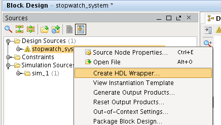 Next we need to generate the Verilog code for the system. Do this by right-clicking on the stopwatch_system and selecting Generate HDL Wrapper. Make sure that the checkbox letting Vivado manage the update is checked and then click OK. This generates the Verilog code for the whole design.
Adding Constraints
Next go to the Project Manager window and add a constraint file. You can use the constraint file from tutorial 12. You may want to change the name. I used stopwatch.xdc.
You should now be able to synthesize the design and generate a bitstream. Go ahead and program the device. Right now the FPGA doesn’t do anything. For that we need to add some ARM software which we will cover in the next tutorial.
Hi,
I am getting the following error messages during Implementation:
[Place 30-58] IO placement is infeasible. Number of unplaced terminals (48) is greater than number of available sites (0).
The following Groups of I/O terminals have not sufficient capacity:
IO Group: 1 with : SioStd: LVCMOS18 VCCO = 1.8 Termination: 0 TermDir: In RangeId: 2 has only 0 sites available on device, but needs 48 sites.
Term: s00_axi_wdata[0]
Term: s00_axi_wdata[1]
Term: s00_axi_wdata[2]
Term: s00_axi_wdata[3]
Term: s00_axi_wdata[4]
Term: s00_axi_wdata[5]
Term: s00_axi_wdata[6]
Term: s00_axi_wdata[7]
Term: s00_axi_wdata[8]
Term: s00_axi_wdata[9]
Term: s00_axi_wdata[10]
Term: s00_axi_wdata[11]
Term: s00_axi_wdata[12]
Term: s00_axi_wdata[13]
Term: s00_axi_wdata[14]
Term: s00_axi_wdata[15]
Term: s00_axi_wdata[16]
Term: s00_axi_wdata[17]
Term: s00_axi_wdata[18]
Term: s00_axi_wdata[19]
Term: s00_axi_wdata[20]
Term: s00_axi_wdata[21]
Term: s00_axi_wdata[22]
Term: s00_axi_wdata[23]
Term: s00_axi_wdata[24]
Term: s00_axi_wdata[25]
Term: s00_axi_wdata[26]
Term: s00_axi_wdata[27]
Term: s00_axi_wdata[28]
Term: s00_axi_wdata[29]
Term: s00_axi_wdata[30]
Term: s00_axi_wdata[31]
Term: s00_axi_araddr[2]
Term: s00_axi_araddr[3]
Term: s00_axi_araddr[4]
Term: s00_axi_awaddr[2]
Term: s00_axi_awaddr[3]
Term: s00_axi_awaddr[4]
Term: s00_axi_wstrb[0]
Term: s00_axi_wstrb[1]
Term: s00_axi_wstrb[2]
Term: s00_axi_wstrb[3]
Term: s00_axi_aresetn
Term: s00_axi_arvalid
Term: s00_axi_awvalid
Term: s00_axi_bready
Term: s00_axi_rready
Term: and s00_axi_wvalid
[Place 30-99] Placer failed with error: ‘IO Clock Placer failed’
Please review all ERROR, CRITICAL WARNING, and WARNING messages during placement to understand the cause for failure.
The constraints file I am using is the one you suggested. The code is also exactly as you posted here.
Thanks,
Frank.
Didn’t register for this thread, registering now.
Full error log at https://codeshare.io/50xggg
Francesco, Sorry I didn’t see that you had posted a comment here until just now. It looks like you are trying to connect an AXI interface to the chip IOs. You don’t want to do this. I will need to fire up the tutorial and see what the issue might be. That would have to wait until this weekend though. What version of Vivado are you using?
Hi Pete,
I solved the problem. It was indeed what you mentioned. Thanks.
HI Francesco Restuccia
could you pl tell me how you resolved that problem mentioned above.
thanks & regards
mayank
Mayank,
The issue was that Francesco had connected the AXI interface to the external pins of the FPGA. This is almost certainly not what you want to do. His solution was to connect them to the appropriate internal IP block. The AXI signal are meant to interconnect IP components within the block design.
If you can be more specific about the problem you are seeing, then maybe I can help.
Thanks,
-Pete
Hi Pete thank you for giving me your precious time
but i am not assigning any axi pin to any chip i/o pin. it automatically takes at implementation and give error :
[Place 30-58] IO placement is infeasible. Number of unplaced terminals (46) is greater than number of available sites (0).
The following Groups of I/O terminals have not sufficient capacity:
IO Group: 1 with : SioStd: LVCMOS18 VCCO = 1.8 Termination: 0 TermDir: In RangeId: 2 has only 0 sites available on device, but needs 46 sites.
Term: s00_axi_wdata[0]
Term: s00_axi_wdata[1]
Term: s00_axi_wdata[2]
Term: s00_axi_wdata[3]
Term: s00_axi_wdata[4]
Term: s00_axi_wdata[5]
Term: s00_axi_wdata[6]
Term: s00_axi_wdata[7]
Term: s00_axi_wdata[8]
Term: s00_axi_wdata[9]
Term: s00_axi_wdata[10]
Term: s00_axi_wdata[11]
Term: s00_axi_wdata[12]
Term: s00_axi_wdata[13]
Term: s00_axi_wdata[14]
Term: s00_axi_wdata[15]
Term: s00_axi_wdata[16]
Term: s00_axi_wdata[17]
Term: s00_axi_wdata[18]
Term: s00_axi_wdata[19]
Term: s00_axi_wdata[20]
Term: s00_axi_wdata[21]
Term: s00_axi_wdata[22]
Term: s00_axi_wdata[23]
Term: s00_axi_wdata[24]
Term: s00_axi_wdata[25]
Term: s00_axi_wdata[26]
Term: s00_axi_wdata[27]
Term: s00_axi_wdata[28]
Term: s00_axi_wdata[29]
Term: s00_axi_wdata[30]
Term: s00_axi_wdata[31]
Term: s00_axi_araddr[2]
Term: s00_axi_araddr[3]
Term: s00_axi_araddr[4]
Term: s00_axi_awaddr[2]
Term: s00_axi_awaddr[3]
Term: s00_axi_awaddr[4]
Term: s00_axi_wstrb[0]
Term: s00_axi_wstrb[1]
Term: s00_axi_wstrb[2]
Term: s00_axi_wstrb[3]
Term: s00_axi_aresetn
Term: s00_axi_arvalid
Term: s00_axi_awvalid
Term: s00_axi_bready
Term: s00_axi_rready
Term: and s00_axi_wvalid
tool is vivado 2016.1
Hi Pete i got problem
actually not clicking on Generate Block Design .
as it was not stated in tutorial
thanks
mayank
These should not be connected at the top level. Make sure your block design looks like the completed one in the tutorial.
just a note, vivado 2018.1 likes to add a “_0” to your external port names e.g. ssd_0. you also need to disconnect the stopwatch clk. After this the bitstream will compile