
When the synthesis and implementation tools run, they need to understand the timing of the design. At a minimum, this means the clock frequency that the design runs at. In most designs there will be more than one clock, so each clock needs to be specified, and the relationship between the clocks needs to be described. In addition, the timing information on input pins and output pins also needs to be communicated. This information is communicated in the form of timing constraints in an XDC file.
Getting Started
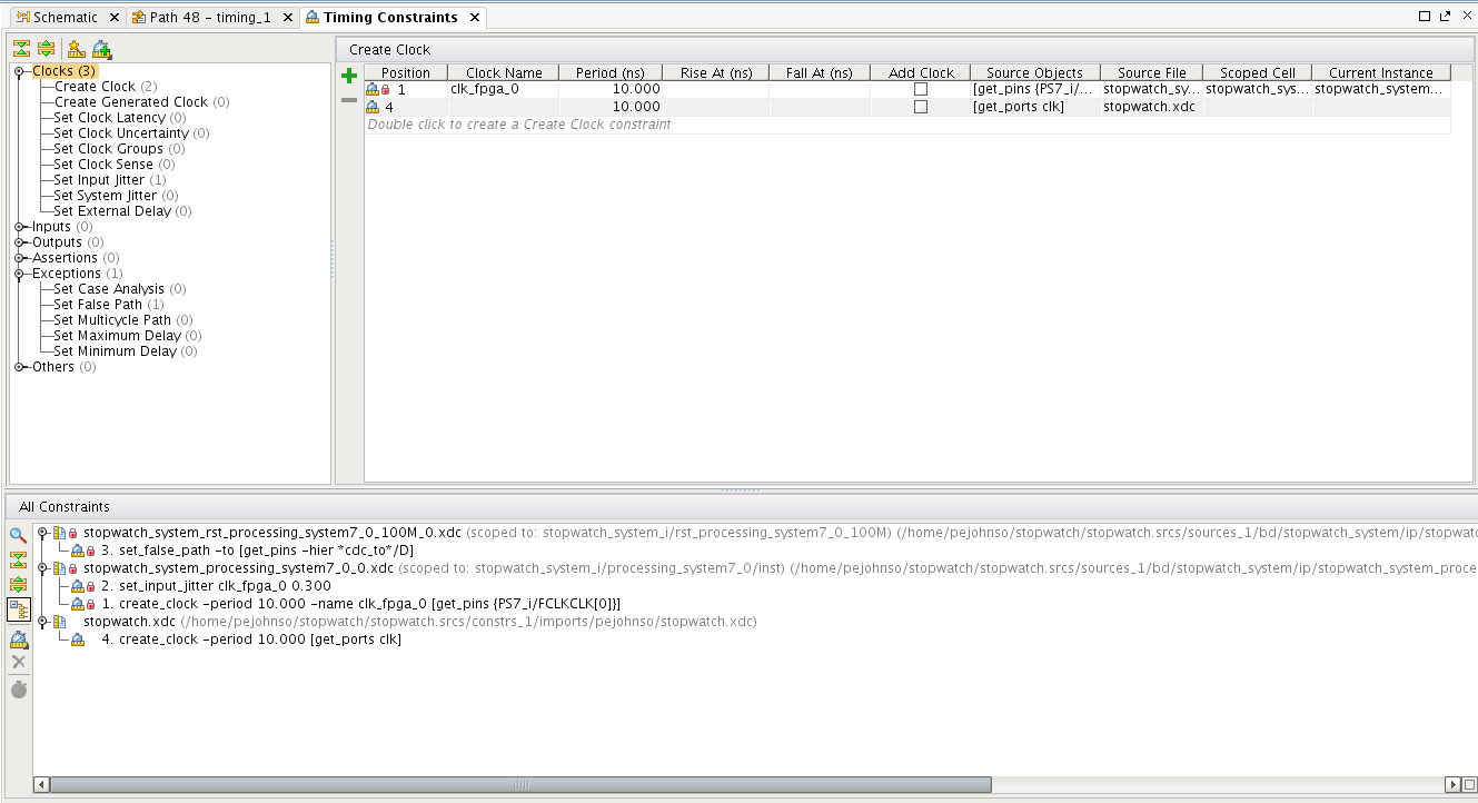 Go ahead and edit the stopwatch design from tutorial 14. Run synthesis and open the synthesized design. Click on the Edit Timing Constraints flow in the Flow Navigator. This should bring up the Timing Constraints window, where you can view and edit timing constraints. The screen should look like the figure to the right.
You should see four timing constraints. Three of them will have little lock symbols next to them. The ones with the lock are generated by the IP Integrator when we built the ARM subsystem. You can see that one is the following:
create_clock -period 10.000 -name clk_fpga_0 [get_pins {PS7_i/FCLKCLK[0]}]
This creates a clock constraint on the AXI logic outside the processor subsystem. Coincidentally, this happens to be the same period as the external clock we use on the clk input. In fact, we could make our lives much simpler if we removed the clock input altogether and just used the clock from the processor to run our stopwatch logic. But if we did that, we couldn’t talk about all kinds of interesting issues in this tutorial.
Notice that we also see the clock constraint on the clk input pin that we put in our XDC file:
create_clock -period 10.000 [get_ports clk]
Running a timing report
Now, click on the Report Timing Summary flow in the Synthesized Design. This will bring up a Report Timing Summary dialog. Use the  default results name and click OK. You should see a timing summary panel open up that looks something like the figure to the right. You’ll probably see some items in red. These are where timing failures exist.
 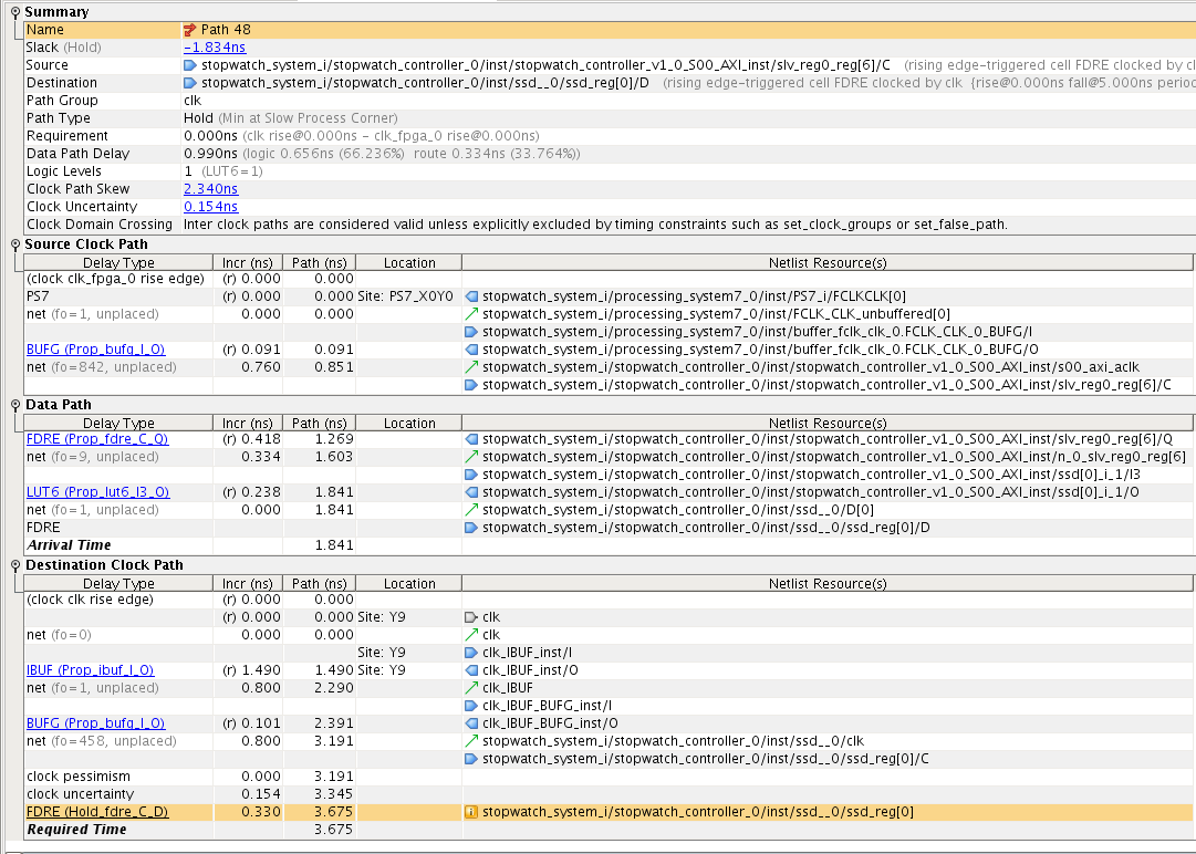 Drill in to the Inter-Clock Paths entry. You’ll see there are hold time violations on signals passing from the clk_fpga_0 clock to the clk clock domain. In my design, there are seven failing paths and the total hold slack is -12.838ns. If you click on the red Hold line, you’ll see the seven failing paths to the right. Double-click on the first line to bring up detailed information about that path. It should look something like the figure to the right.
Interpreting the results
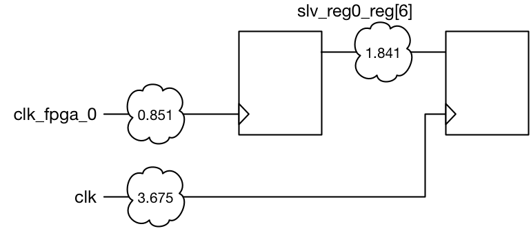 What does this information mean? Well, first of all, this is a hold time violation. Consider the figure to the right. The timing tool thinks that the two clocks are identical, since they are both 100MHz, and because they both rise 0ns into the period. It looks at the delay in the clock tree going to the source flip-flop of 0.851ns. Then it looks at the delay through the logic to the destination flip-flop of 1.841ns. It then sees a delay of 3.675ns on the clock tree of the destination flip-flop. The timing tool will see this situation as a hold error, since when both clocks rise, the data clocked in to the source flip flop will actually race through the logic and arrive into the destination flip-flop too soon. The source flip-flop has not held the data stable for long enough.
Thinking about the problem
What does this error mean? First of all, the tool is wildly wrong about its assumptions. While both clocks are 100MHz, they don’t come from the same oscillator. This means they are not harmonically related. In lay terms, this means that they are really not exactly 100MHz, but are off a tiny amount, in different amounts. This means there really isn’t any timing relationship between the clocks. What does this mean for our design? This path is data from the processor which is going to be displayed on the seven segment display– which a human will look at. This data doesn’t change very often, and if it is wrong for 10ns when it does, nobody will notice.
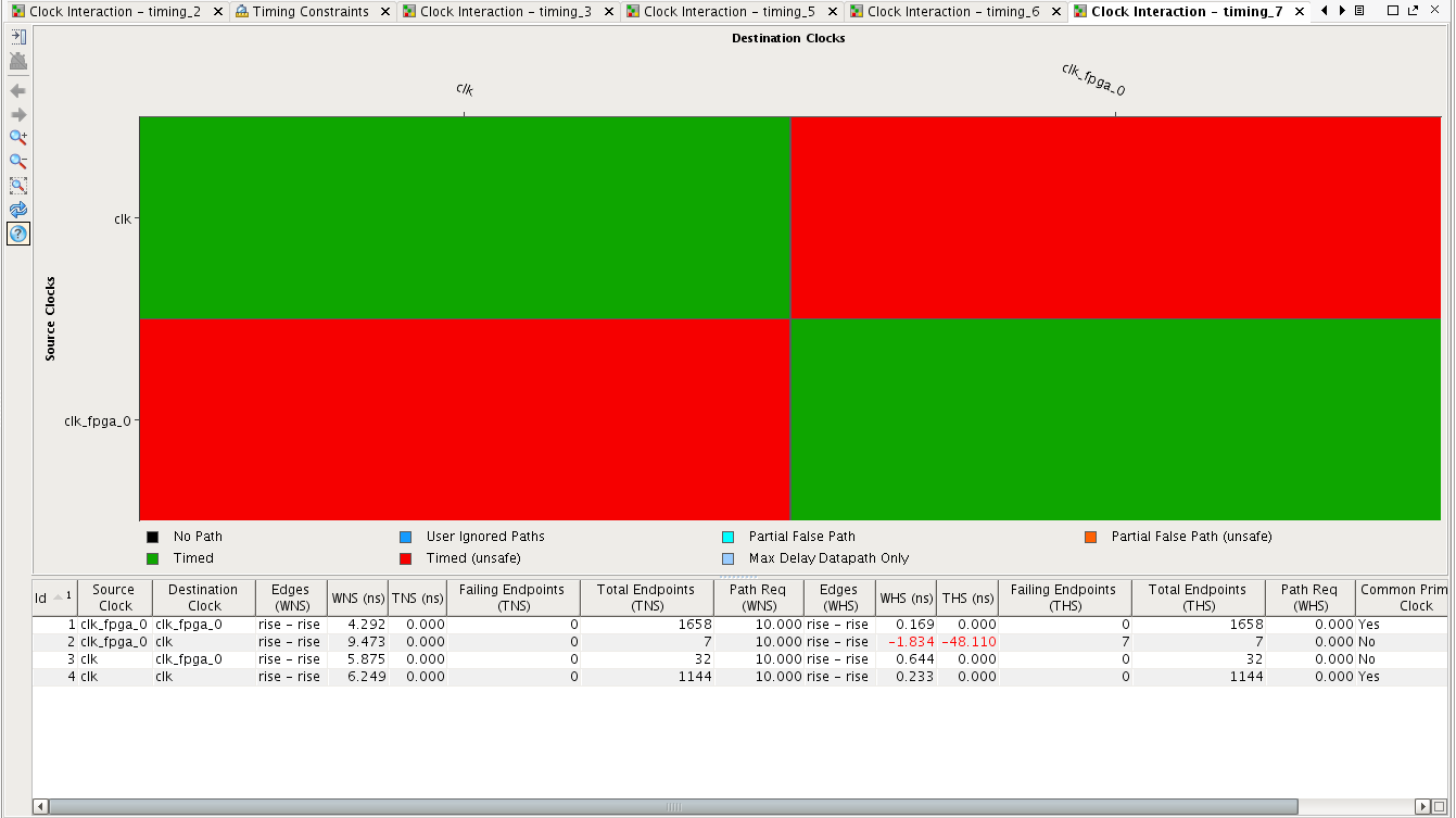 Another report which is good to run now helps you visualize the situation. Go ahead and click on the Report Clock Interaction flow. This should bring up a panel like the one shown to the right. The panel shows the status of paths, depending on source clock and destination clock. The green shows that both paths fully within each of the two clock domains are Timed. This means they are checked and everything looks good. Paths between clock domains are checked, but there are still problems. This is what we’re going to need to fix.
Resolving the problem
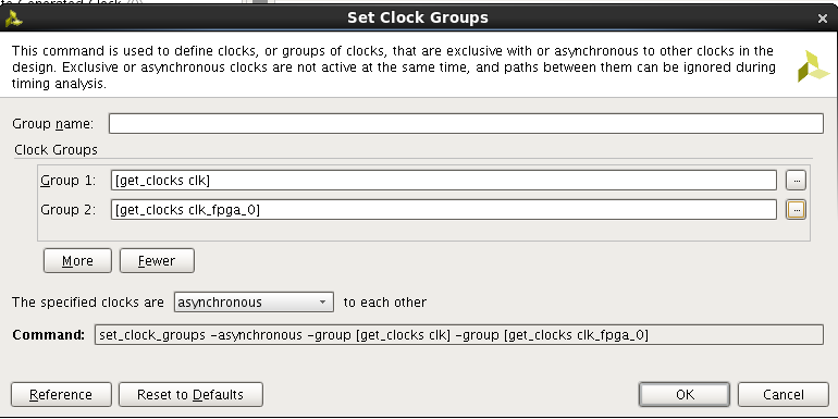 There are two ways we can go about resolving this problem. First, we can tell the synthesis tool that the clocks are asynchronous. You can go into the Edit Timing Constraints flow and create a clock group. Add both clocks to the group, then specify that the clocks are asynchronous to each other. This would look like the figure to the right. You can even see the XDC command to specify this relationship:
set_clock_groups -asynchronous -group [get_clocks clk] -group [get_clocks clk_fpga_0]
The problem with this approach is that it works too well. It basically tells the timing tool, “hey, anything going between these clock domains is hopeless, so don’t bother looking at it”. This may be true, but perhaps we should be more explicit about what should be ignored.
The second solution is to create a false path. The false path tells the timing analyzer to ignore this timing path because we don’t care what happens here.
Go back to the Timing Constraints editor and select the Set False Path entry under Exceptions. Click the green plus button to create a new false path. We will need to specify a source for the false path and a endpoint for the path. We will be using wildcards to help simplify the constraint, which will reduce the total number of constraints. Click the … button to the right of the From line. For the pattern enter *slv_reg0_reg[*]/C, check the Search hierarchical box, then click the Find button. Specify the clock pin on the flip-flop as the source point for the false path. You should see the 32 source points show up in the Find results window. Click OK. Now, click the … button next to the To line and check the Search hierarchical box. Search for *ssd_reg[*]/D and click Find. You should see the seven ssd registers appear. Then click OK.
You should see a XDC command that looks like this:
set_false_path -from [get_pins {*slv_reg0_reg[*]/C} -hierarchical] -to [get_pins {*ssd_reg[*]/D} -hierarchical]
Go ahead and click OK. Now go to the file menu and save the constraints. You can rerun synthesis or, since we just changed the constraints, you can just force the synthesis to be up to date. If you update the timing summary, you should see the hold violations go away. Also, you should rerun the Report Clock Interaction flow. You should now see that the data from the fpga_clk_0 domain to the clk domain is all blue (User Ignored Paths).
Implement the design
So far we’ve been running the timing reports on just the synthesized design. All of the numbers in the report are just gross estimates. There has not yet been any placement or routing of the design. Go ahead and implement the design. We’re then going to run some reports with more accurate numbers.
Analyzing the implemented design
Open up the implemented design and run a Report Timing Summary. You should see no red entries, which indicates that we have passed our timing checks. To the left of the timing summary window, you will see a hierarchical list of paths within the design. Notice that the last one is Unconstrained Paths. Go ahead and drill down into that list. You will see three sub-categories, clk to NONE, clk_fpga_0 to NONE, and NONE to clk. 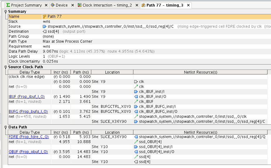 This is basically a list of things that we have overlooked. Paths that have not been constrained. These are freebies to the place and route tool, but do we care about these paths? The first list clk to NONE are the ssd output pins. These come from the clk clock and go off chip. If you click on Setup you will see a list of the longest paths in this category. In my design the longest path is from ssd_reg[4] to ssd[4]. The total delay on the path is 9.067ns. If you double click that path, you will see a detailed description of what is on the path. Mine is shown in the figure to the right.
The path is broken into two parts. The first is the clock insertion path. You can see the clock come on the chip and go through the input buffer (the IBUF) go through some wiring, and then go through a global buffer (BUFG) and then through more wiring. The total time for that is 5.415ns. The next section is through the flip-flop and off the chip. It takes 0.518ns to go through the flip-flop (FDRE) and then 4.955ns of wiring delay, and then 3.595ns to go through the output buffer (OBUF). The grand total on this delay is a whopping 14.483ns.
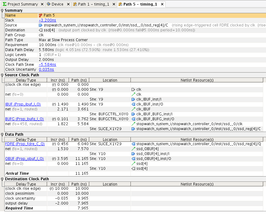
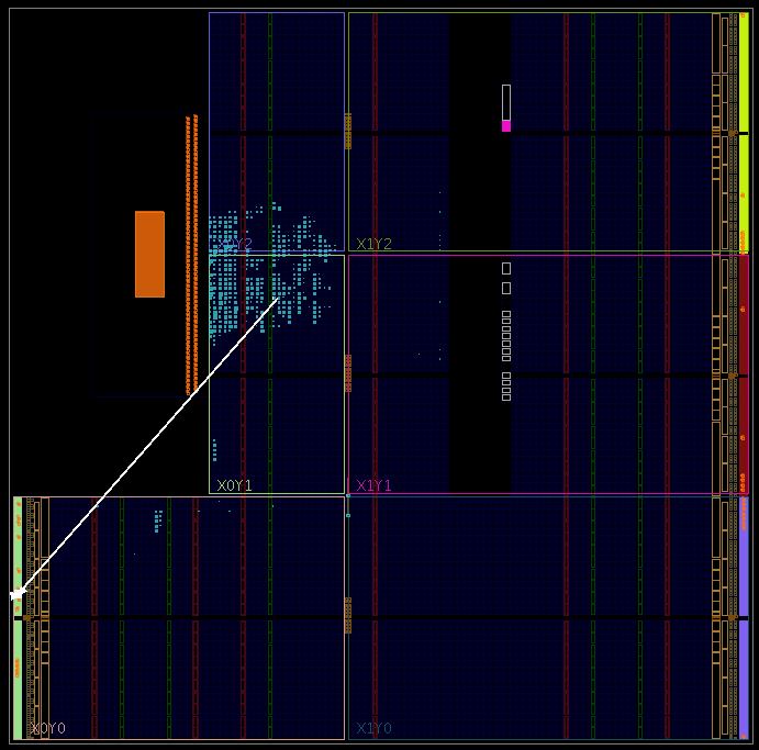 Go ahead and click on the Device tab above the timing path summary. You will see a floorplan of the chip and the path we are looking at will be highlighted. Here is what my design looks like. Notice that that path goes all the way across the chip. Now in our case this is an SSD that a person is looking at. 15ns may seem like a long time on the FPGA world, but a person will not be able to tell the difference if it was even a million times that long. But suppose we do care. If this signal was going to another chip this might be an issue.
Constraining the output
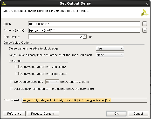 Let’s go back to the Edit Timing Constraints flow under the Implementation flow. We are going to set an output delay on the ssd output. Click on the Set Output Delay line. Then, click the green plus sign to create a new constraint. Fill in the constraint as shown in the figure to the right. This specifies that we only want at most 2ns of output delay on the path. Your command should look like this:
set_output_delay -clock [get_clocks clk] 2.0 [get_ports {ssd[*]}]
Click Apply, then save the constraints. Go ahead and rerun the implementation. This will synthesize and place and route with the new output constraints.
The value you use for the set_output_delay command is a little backwards from what you might expect. You should think of the number as meaning the amount of delay outside the chip that the signal needs to go through before being clocked into a flip-flop outside the chip on the same clock.
The new results
 After the implementation completes, you will notice that the new design failed timing. Go ahead and run a Report Timing Summary again to see what happened. If you look at the path you will see that the net delay between the flip-flop and the output buffer is greatly reduced from 5.4ns to 1.5ns.
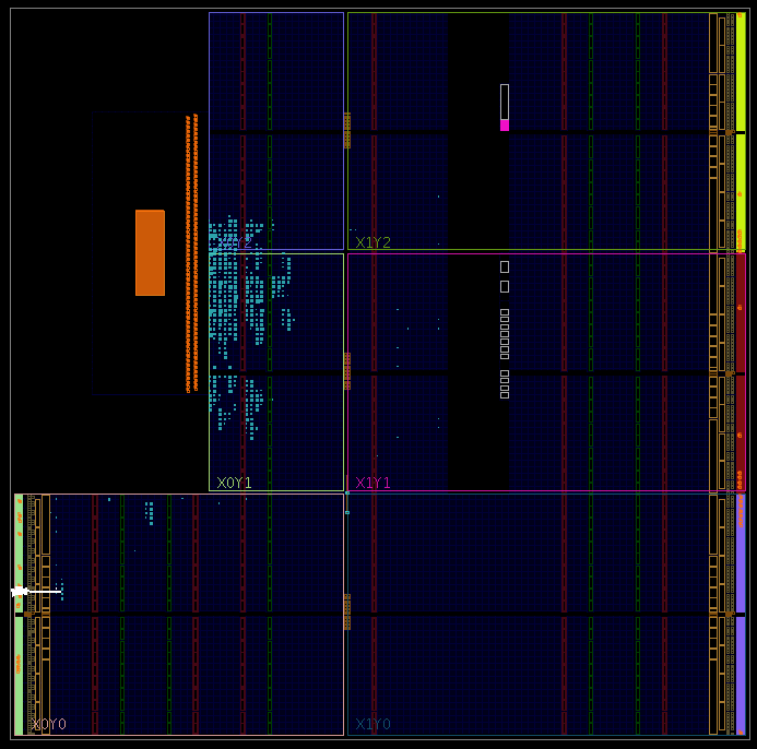 Let’s look at the layout. Select the Device tab again and you will see the path highlighted in the new implementation. As you can see from the figure, the path is now much shorter. The place and route tool has taken in the constraint information and changed its strategy for meeting our constraints. But still, the clock insertion delay is really causing us grief.
In a design where our output timings mattered, we could use a PLL to remove the insertion delay of the clock. But that is really overkill in this situation.
Specifying a maximum delay
Go ahead and remove the set_output_delay constraint on the ssd output. Then create a Set Maximum Delay constraint. You will find that under the Exceptions category. The From point should be the clk net and the To point should be the ssd[*] ports. The final constraint should look like this.
set_max_delay -from [get_clocks clk] -to [get_ports {ssd[*]}] 8.0
Click the Apply button, then click the link to rerun the static timing. Notice that you can change timing constraints and then simply rerun the static timing tool. This will reanalyze the design but the new constraints will not have any effect on the implementation of the design. Once you reimplement, the constraints are viewed as goals by the synthesis and place and route algorithms.
You will see that the paths are still failing. In effect, we really haven’t changed anything. The set_max_delay value of 8 is pretty much the same as the set_output_delay value of 2 when the clock is 10ns. Notice however that you can edit the constraint in a spreadsheet mode after it is created. Just select the set_max_delay constraint and you will see above that you can make changes to the value and other properties. In particular, we want to check the Data Path Only option. Go ahead and check this and also change the delay value to 6. Your constraint should now look like this.
set_max_delay -datapath_only -from [get_clocks clk] -to [get_ports {ssd[*]}] 6.0
Click Apply again and rerun the timing analysis. You should now see the static timing pass. The set_max_delay constraint is now not considering the clock insertion delay but only the delay from the flip-flop to off chip.
Look through the other unconstrained paths and add set_max_delay constraints for the other outputs. I added constraints for ssdcat and for led[*]. Note that since the LED outputs are driven from the ARM directly they use a different clock. Notice how the ssdcat output meets timing, but the LED outputs do not. I suspect that the logic for the ssdcat output got grouped with the other ssd logic so it happens to meet timing now. The LED logic however doesn’t. If you resynthesize and reimplement the design, the LED output should now meet timing.
Input delays
We still have more unconstrained paths. If we look through those we see that we don’t have constraints on our input switches and buttons. Go ahead and add set_max_delay constraints there of 2.5ns. Here are the constraints that I have:
set_max_delay -from [get_ports {btn[*]}] 2.500
set_max_delay -from [get_ports {switch[*]}] 2.500
set_max_delay -from [get_ports enc_a] 2.500
set_max_delay -from [get_ports enc_b] 2.500
set_max_delay -from [get_ports enc_btn] 2.500
set_max_delay -from [get_ports enc_sw] 2.500
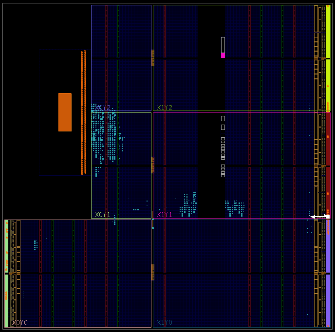 Notice how I only have the start of the path specified. This is enough to identify these paths. Save the constraints and reimplement the design. After completing the place and route, the design now meets timing. I have included the new floorplan for the design. Notice how we are starting to see logic move to different locations in the chip? My floorplan is shown to the right and you can see the path for btn[3] highlighted. The path is now quite short, and the synchronization flip-flop is located near the IO pin.
Investigating more unconstrained paths
Let’s continue through our list of other unconstrained paths. In the NONE to clk_fpga_0 category we see some from switch_out_reg in the debounce logic to the slave register in the AXI register block. Add a max_delay of 5ns on those paths. Rerun the timing. Notice that each time you run the timing, it only reports the 10 longest paths in each category. So it looks like we are starting to play whack-a-mole with constraints. If you click on the Report Timing Summary flow to rerun timing, it will bring up a panel where you can set options for the timing run. You can see under Path Limits where you can set the Maximum number of paths per clock or path group. Change that to 100 and rerun the timing. Now we can see more of the paths in one report.
There are also some paths from the encoder and from the timer counter to the AXI registers. Now these paths don’t come from asynchronous user inputs, so we should not dismiss them so easily
Hi Pete, you mention that “create_clock -period 10.000 -name clk_fpga_0 [get_pins {PS7_i/FCLKCLK[0]}]” creates “a clock constraint on the AXI logic outside the processor subsystem”. How does one deduce that this constraint is for the AXI logic outside the processor subsystem?
Because it is coming out of the ARM processor. If you configure the ARM IP you will see where you configure the output clocks. The default is for there to be one clock running at 100MHz.
hi Pete Johnson,
what does this line means to? :
create_clock -period 10.000 [get_ports clk]
why we are putting constraint on clk
Actually you are putting constraints on the logic which uses the clock. You are telling the synthesis system that the logic has 10ns to go from the source clock edge to the destination clock edge.