
I2S Loopback
In this tutorial, we’ll build an FPGA that loops the I2S receive data back to the I2S transmitter. Basically, an even more complicated wire. Don’t worry– in our next tutorial, we’ll be doing some processing on the data inside the FPGA.
Packaging the transmitter and receiver IP
If you still have the Vivado projects from doing the IP transmitter and receiver, you should open the receiver up now. If not, you should create a new Vivado project containing only the I2S receiver design.
You should see something like the following figure in your Project Manager view: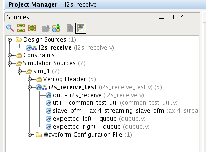
Notice that the i2s_receive module is in the Design Sources section. This means that it’s part of your FPGA design. It is also in the simulation sources view as well. But there are other files there as well, which compose the other simulation files.
Go to the Tools menu and select Create and Package New IP. Click Next, make sure the Package your current project option is selected, then click Next again. Select a location for your IP repository and click Next. You should use the same location when creating both the I2S transmitter and receive packages. A dialog box will appear, asking for you to Confirm Copy Sources. This lets you know that the source files for the IP will be copied to the IP repository. Go ahead and click OK.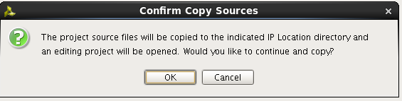
You should now click Finish on the Create and Package New IP dialog.
Vivado seems to get a little confused and tries to use the simulation test as the IP top module. I get a message which looks like this. You will not see this if your project has no simulation files.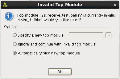
Simply check the Specify a new top module option and select i2s_receive as the top module and click OK.
You should now see the IP packager windows, like we have seen before: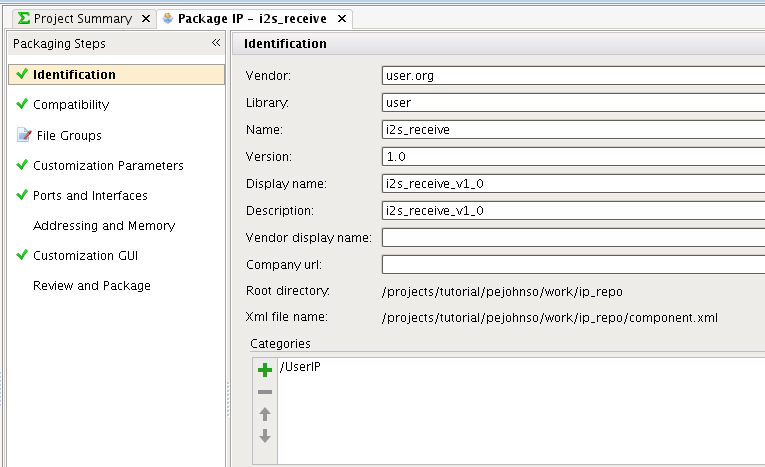 All that we need to do is select File Groups and click the Merge changes from File Groups Wizard link.
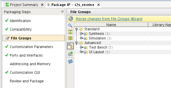 Then select the Review and Package tab and click Re-Package IP. This will return you to your previous project.
Repeat these steps to create an IP package for the I2S transmit design.
Creating the loopback design
Make a copy of your design from tutorial 17 and open the design. We are going to modify the design to add the I2S receive and transmit blocks.
Go ahead and add the i2s_receive and i2s_transmit IP blocks to the design. You may need to use the modify the IP portion of the Project Settings to point to your IP repository directory where you stored your i2s_receive and i2s_transmit IP blocks.
After adding the i2s_receive and i2s_transmit blocks you need to connect the adau1761_bclk input pin to the sck ports of the two IP blocks. Also connect the adau1761_lrclk pin to the ws inputs. Connect adau1761_adc_sdata to the mosi input of the i2s_receive IP block, and the adau1761_dac_sdata output port to the miso output of the i2s_transmit block. Your final block design should look like this: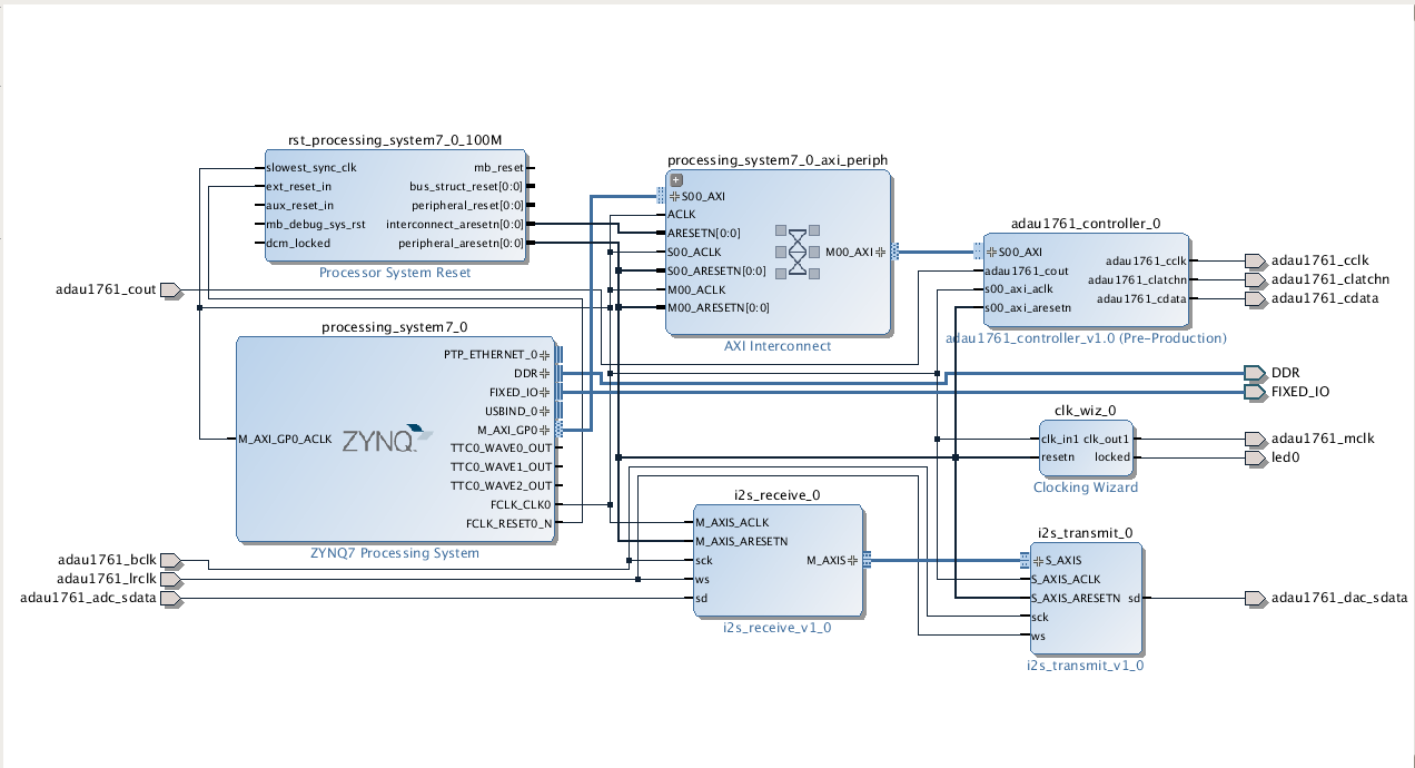
Synthesis
Before we synthesize the design, we need to add an additional constraint. If you recall from tutorial 19, the sd output was actually clocked from the falling edge of sck. Normally, when presented with a clock signal, the place and route tools try to create a balanced clock network using special clock resources in the FPGA. Part of this network is a low-latency path from the clock input pin to the clock network. Not all input pins have this ability, and only a few can be used as a global clock. If we try to synthesize the design as-is, we will get an error saying that the clock input pin adau1761_bclk is not on a dedicated clock pin. We’re going to need to override this error by using the following constraint:
set_property CLOCK_DEDICATED_ROUTE FALSE [get_nets adau1761_bclk_IBUF]
By setting this constraint, you’re basically indicating that you understand there will be some additional delay associated with not using a dedicated clock input pin. This is OK in our situation, since the clock will only be going to a single flip-flop, and if there is an extra few nanoseconds of delay on that path, it really doesn’t matter.
After adding the constraint, you should be able to place and route the design and create a bit file. Program the FPGA as with tutorial and export the design to SDK. You can use the same software from tutorial 17 to test the design.
Hi Pete,
1) I have connected M_AXIS of i2sreceive block to DRAM Memory. And start a transfer of 8 bytes to memory through C and in the interrupt handler, I continue the transfer of next 8 bytes to memory until i store the required number of audio bits. I am getting data only for the first transfer in many cases and sometimes 2 or more but not in consecutive memory locations. Am I making any mistake here? Since DRAM memory is also a streaming interface, shouldn’t the data get copied to memory without any problems? Should i make any change to the tready signal which is currently input to the i2sreceive block? Please note i don’t have the i2s transmitter connected.
2) I have connected M_AXIS of i2sreceive block to a FIFO(So that 256 samples get buffered before it is fed to fft) and then to 256 point FFT streaming module and then connect it to memory. I get no data in memory. Can you suspect what mistake I am doing?
I am a beginner in FPGA and I am stuck with this from 2 weeks.
I’m on vacation right now. But it sounds like another commenter on tutorial 21 is working on DMA as well. Maybe you can help each other.