
In this tutorial, we’re going to take a diversion from the I2S audio and look at embedded Linux. Up until now, we’ve been using bare metal programming for the ARM. This is the easiest method of programming the ARM for simple tasks, but once we want to start doing things which are complicated, it’s good to get an operating system involved. In this tutorial, we will be using the Petalinux tools recommended by Xilinx.
Requirements
Before proceeding further you need to make sure that you have installed Xilinx Vivado 2015.4 and the Xilinx Petalinux 2015.4 tools. It is helpful if the Vivado and Petalinux versions match, and 2015.4 seems to be the latest stable release as I write this. As time moves on, you may want to try this with other newer releases. If so, you can expect some subtle differences between the tools you use and this tutorial.
I install the Petalinux tools and Vivado tools into the same directory on my machine. This is not a requirement, but it keeps things organized. I also use the path /tools/xilinx, so my Vivado install is in /tools/xilinx/Vivado/2015.4 and my petalinux install is in /tools/xilinx/petalinux-v2015.4-final.
Note that the Petalinux tools only run under Linux, so if you have been using Windows for Vivado, you need to switch to Linux, or you’ll need to adapt these instructions for building on two different machines.
Building the FPGA Design
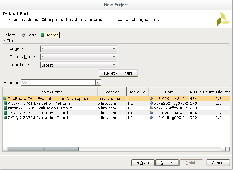
We first need to build an FPGA design to program into the ZYNQ part. Don’t worry if you have not followed along with the previous tutorials. In this tutorial, you will not need to write any Verilog code. Start Vivado– you may need to source the appropriate settings file to set the environment for your shell. Once Vivado is started click Create New Project. This starts the Create New Project Wizard. Click Next and enter the project name zedboard_spi and then click Next again. Click Next again to create an RTL project, and then click Next again because we don’t need to add any sources. Click Next once again, since we’re not adding existing IP, and click Next because we are adding no constraints. Finally on the Default Part page, click Boards and select the ZedBoard, then click Next.
Finally, click Finish to create the project.
In the Flow Navigator panel, click Create Block Design to start a new block design. Name the design system and click OK. The design will be empty, so click the add IP button to start adding IP. Note that you can mouse over the buttons to see what they are named. Select the ZYNQ7 Processing System and press Enter. This will add the processing system to the FPGA. Click the add IP button again, and add an AXI GPIO block. Add three more AXI GPIO blocks for four total. Click the Regenerate Layout button to organize the diagram.
Now, click the Run Block Automation link at the top of the window. This will configure the ARM processors for use on the ZedBoard FPGA board. Click OK. Notice that connections for the DDR memory and FIXED_IO have been added.
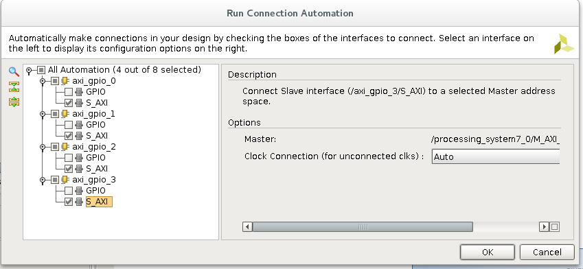
Now click the Run Connection Automation link. Select the S_AXI connections for each of the four GPIO blocks, then click OK.
Now click the Regenerate Layout button to clean up the diagram. Notice that a Processor Reset System unit and an AXI Interconnect unit were automatically added and connected. This logic allows the ARM processors to talk to the FPGA GPIO units. We’re still going to need to connect the GPIO units to some external pins, however.
We will connect one GPIO unit to the eight LED outputs, one to the eight switch inputs, one to the five pushbutton inputs, and finally, one to the JA1 Pmod connector, which we will use as a SPI interface.
Click the Run Connection Automation link again. Notice how the AXI options have gone away but we can still select the GPIO connections. Select the axi_gpio_0 unit to connect to btns_5bits, the axi_gpio_1 to leds_8bits, the axi_gpio_2 to sws_8bits, and the axi_gpio_3 to connect to Custom.
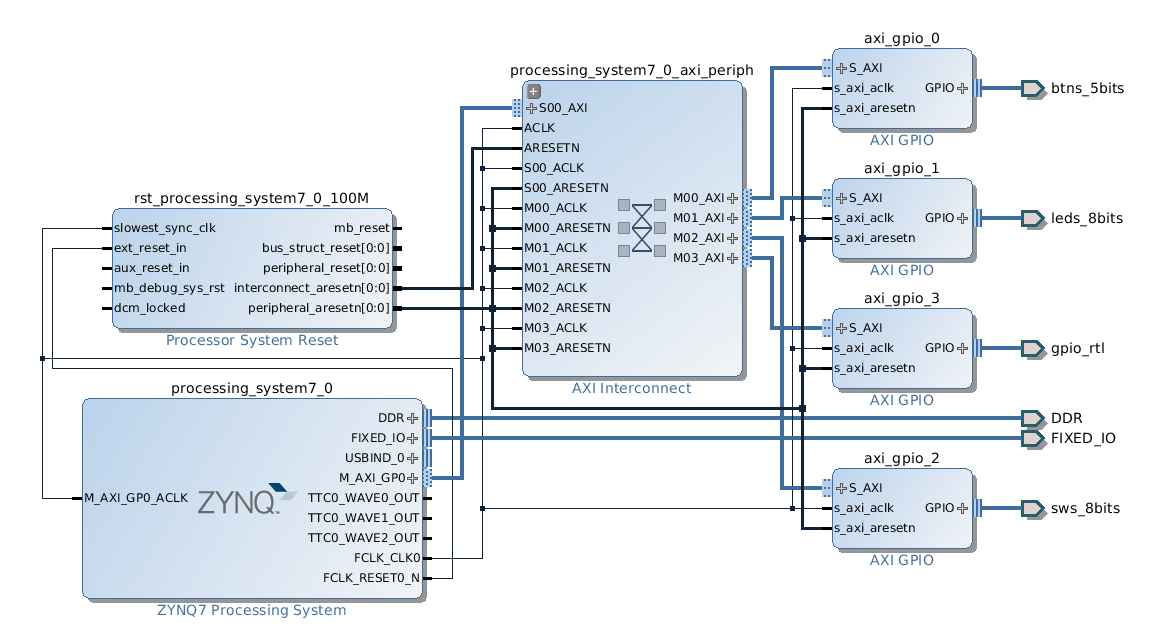
You should have a diagram that looks something like this:
Double-click on the axi_gpio_0 block. Then select the IP Configuration tab. Notice that the width has been set to 5 bits and the All Inputs box has been checked. The connection automation knew that the buttons were five bits and that they could only be inputs. The leds GPIO has been set to eight outputs, and the switches have been set to eight inputs. Go ahead and click Cancel. Double-click on the axi_gpio_3, which is connected to gpio_rtl, and you can see that it is configured for 32 bits and bidirectional operation. Go ahead and set the width to eight, then click OK.
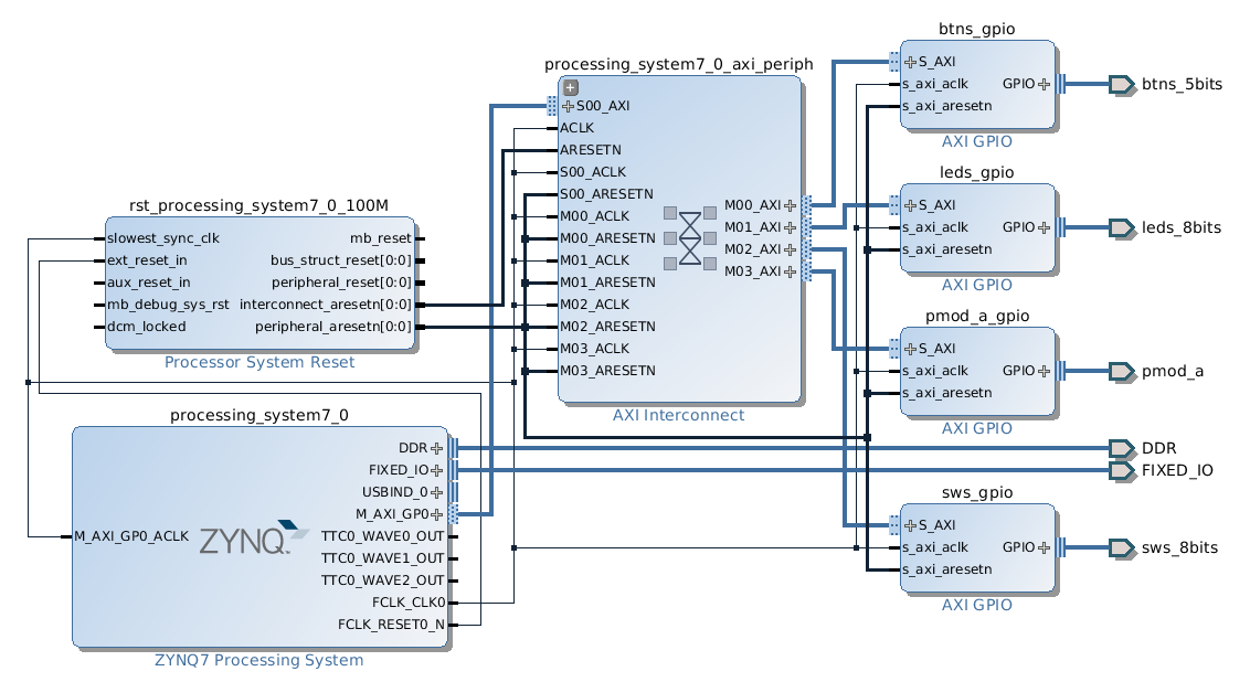
Change the name from gpio_rtl to pmod_a, and change the names of the axi_gpio_0 block to btns_gpio. Likewise, change the other names as well. Your final diagram should look like this:
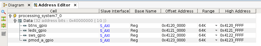
Click on the Address Editor tab and drill down to the address mapping for the FPGA. It should look like this:
Go back to the Diagram tab and click the Validate Design button. The design should validate successfully.
Now go ahead and click on the Generate Block Design task in the IP Integrator section of the Flow Navigator (way to the left). The Generate Output Products dialog will pop up. Click the Generate button. It may take a few seconds for this dialog to pop up, so be patient. This process builds the RTL code for the block design that you have just entered.
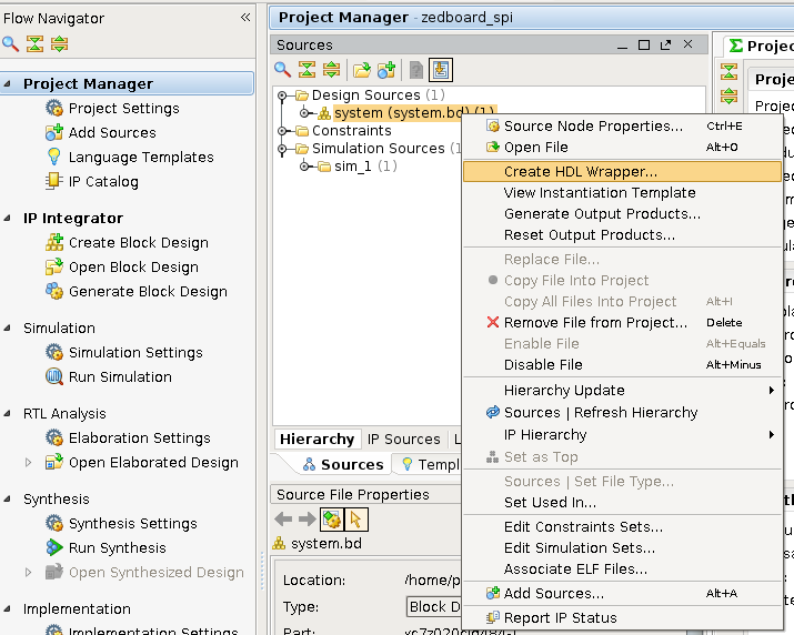
Now, we’ll leave the IP Integrator and select the Project Manager. In the Design Sources section you can see the block diagram that we created. Right clock system and select Create HDL Wrapper… This will build the top level of the FPGA design for us. Make sure to let Vivado manage the update.
Creating Constraints
The FPGA design itself is almost done. We now need to tell Vivado about the Pmod pins. It already knows about the buttons and LEDs from a board description, but we need to tell Vivado which FPGA pins connect to the Pmod port. From the Project Manager section of the Flow Manager, click Add Sources. Select the radio button for Add or create constraints and click Next. Then click Create File and enter the file name system. The file type should be XDC and the location should be local to project. Click OK. Then click Finish to dismiss the Add Sources dialog. If you drill down to the Constraints section of the sources panel, you will see a new constraint file called system.xdc. Double click that file to edit it.
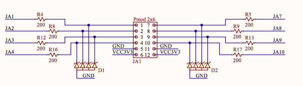
The constraint file will let us map a pin on the FPGA to a port in the design. This will let us connect that port in the design to a pin on the Pmod connector. We first need the ZedBoard schematic. You can see the Pmod connectors on page 3 and the signals are named JA1, JA2, JA3, JA4, JA7, JA8, JA9, JA10 for Pmod connector JA1.
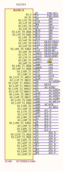 We now need to find where those signals names are connected to the FPGA. The figure has JA2 highlighted, and you can see that it connected to the FPGA pad AA11.
All in all we have the following mapping:
| Signal | Pad |
|---|---|
| JA1 | Y11 |
| JA2 | AA11 |
| JA3 | Y10 |
| JA4 | AA9 |
| JA7 | AB11 |
| JA8 | AB10 |
| JA9 | AB9 |
| JA10 | AA8 |
set_property PACKAGE_PIN Y11 [get_ports {pmod_a_tri_io[0]}]
set_property PACKAGE_PIN AA11 [get_ports {pmod_a_tri_io[1]}]
set_property PACKAGE_PIN Y10 [get_ports {pmod_a_tri_io[2]}]
set_property PACKAGE_PIN AA9 [get_ports {pmod_a_tri_io[3]}]
set_property PACKAGE_PIN AB11 [get_ports {pmod_a_tri_io[4]}]
set_property PACKAGE_PIN AB10 [get_ports {pmod_a_tri_io[5]}]
set_property PACKAGE_PIN AB9 [get_ports {pmod_a_tri_io[6]}]
set_property PACKAGE_PIN AA8 [get_ports {pmod_a_tri_io[7]}]
set_property IOSTANDARD LVCMOS33 [get_ports pmod_a_tri_io]
The first eight constraints set the package pin for each bit of the pmod_a port. The final constraint sets the IO type on the port to 3.3V CMOS. Note that this can apply to the entire 8 bits of the port. Also note that, for reasons which likely aren’t very good, Vivado has added a suffix of _tri_io to the port name. It doesn’t do this for inputs or outputs, but it feels compelled to do this for bidirectional pins.
Building the FPGA
Save your constraints file and click Generate Bitstream, located in the Program and Debug section of the Flow Navigator. After a few minutes, you should receive a dialog indicating that the build has completed. Elect to open the implemented design.
Exporting the Design
At this point you can go to the File menu and select Export->Export Hardware. In the dialog, make sure Include bitstream is checked, and that you are exporting local to project. This export saves the design and related files in a location where the Software Design Kit (SDK) can find them.
In the next tutorial we build a custom Linux distribution using the FPGA we built in this tutorial.
On Vivado 2016.4, the sufix “tri_io” didn’t work for me, but the sufix “tri_i” did!!
Maybe they changed the name of the ports that the Create HDL wrapper script generates. Things always drift a little as the tool revisions change. Thanks for the comment.
Also on Vivado 2016.4, the suffix tri_io worked perfectly for me