
Verilog
First, we will make the simplest possible FPGA. It will be a wire. Create a new project in Vivado called tutorial1 and add a Verilog file called top.v. You can use the wizard to add ports if you like when Vivado creates the file, or you can add them yourself using the text editor. The design should have a single input called switch and a single output called led.
Edit the file so it looks like this
module top (
  input switch,
  output led
);

  assign led = switch;
endmodule
This declares a Verilog module called top. A module is just a container for part or all of your design. We will learn later that modules can instantiate other modules to create a hierarchical design. But, given that this is the simplest FPGA in the world, that is not necessary.
We declare the module to have a single input called switch and a single output called led. These will correspond to input and output pins on the actual FPGA. The only thing else in the design is the assignment statement. This statement just means that the output led is to change whenever the input switch changes. In effect, it simply creates a wire and connects led to switch.
Constraints
The compiler cannot turn your Verilog code into a working FPGA however because you have not given it enough information. Sure, it knows there is an input pin called switch and an output pin called led, but which pins do you want to use? There are hundreds to choose from. We need to tell it which pins to use. We call this information constraints because it constrains the compiler– it can’t just pick one, but instead must use the one you constrain it to.
Create an XDC constraints source file and call it top.xdc. You should download a copy of the ZedBoard schematics to determine the constraints. But even so, I have included the important information here.
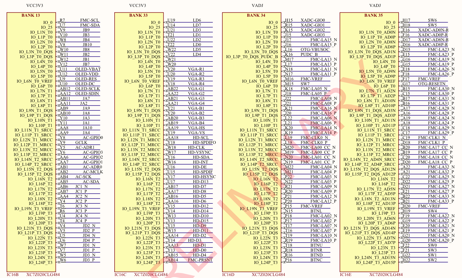
If you look at the schematic, you’ll see that there are eight switches and eight LEDs. Switch 0 comes into the FPGA as SW0 on the schematic and it connects to pin F22 on the FPGA. Notice also that the voltage on the IO bank where the input belongs (bank 35) is VADJ. This voltage is adjustable on the board between 2.5 and 1.8 volts. Assuming your jumper is set to 2.5V, that means this is a 2.5V input.
If you look at the upper left of the schematic you will see a signal called LD0 which is connected to LED 0. This is on a 3.3V bank connected to pin T22. Edit your top.xdc file so that it contains the following constraints. These constraints tell the compiler where we want to connect our inputs and outputs and what logic levels to use for those pins.
set_property IOSTANDARD LVCMOS33 [get_ports led]
set_property IOSTANDARD LVCMOS25 [get_ports switch]
set_property PACKAGE_PIN T22 [get_ports led]
set_property PACKAGE_PIN F22 [get_ports switch]
You should now be able to compile the design. Generate a bit file and program the board. If the blue LED comes on after programming everything should have worked. Slide Switch 0 on and off. The LED should turn on and off as well. Congratulations: you have just created a very expensive and complicated wire!
More Wires
So now let’s modify our design to use a bus of eight wires for the switches and LEDs. since we have eight of those on our board.
Change the Verilog file to
module top (
  input [7:0] switch,
  output [7:0] led
);

  assign led = switch;
endmodule
This will change the inputs and outputs to eight-bit busses. You don’t need to modify the assignment statement. The width of the values just changes from one bit to eight bits. However, the constraints do change a fair amount.
Before, the name of the input pin was switch, and the output pin was called led. Now those values refer to eight pins. We need to apply the PACKAGE_PIN to individual pins. Our constraint files are actually a little program written in the TCL programming language. set_property is a function defined in TCL, and the values passed to it are arguments. get_ports is another function which searches the design database for ports. The square brackets tell TCL to call the function inside them and use the value of the result in place of the brackets. So we can still use the same IO_STANDARD commands. The [get_ports led] call will just return a list of eight ports that match the name led. The set_property command can apply the same IOSTANDARD attribute to all eight. For the PACKAGE_PIN attribute, we need to be more selective. The actual port name for the LSB of the led is led[0]. But we can’t just use this for the name since TCL will try to call a function 0 rather than using the literal characters. We quote the special characters in curly braces. So we will use [get_ports {led[0]}].
Looking at the schematic for all the pin names, we get the following constraints:
set_property IOSTANDARD LVCMOS33 [get_ports led]
set_property IOSTANDARD LVCMOS25 [get_ports switch]
set_property PACKAGE_PIN T22 [get_ports {led[0]}]
set_property PACKAGE_PIN T21 [get_ports {led[1]}]
set_property PACKAGE_PIN U22 [get_ports {led[2]}]
set_property PACKAGE_PIN U21 [get_ports {led[3]}]
set_property PACKAGE_PIN V22 [get_ports {led[4]}]
set_property PACKAGE_PIN W22 [get_ports {led[5]}]
set_property PACKAGE_PIN U19 [get_ports {led[6]}]
set_property PACKAGE_PIN U14 [get_ports {led[7]}]
set_property PACKAGE_PIN F22 [get_ports {switch[0]}]
set_property PACKAGE_PIN G22 [get_ports {switch[1]}]
set_property PACKAGE_PIN H22 [get_ports {switch[2]}]
set_property PACKAGE_PIN F21 [get_ports {switch[3]}]
set_property PACKAGE_PIN H19 [get_ports {switch[4]}]
set_property PACKAGE_PIN H18 [get_ports {switch[5]}]
set_property PACKAGE_PIN H17 [get_ports {switch[6]}]
set_property PACKAGE_PIN M15 [get_ports {switch[7]}]
Make these changes, generate a new bit file, and program the board and now all the switches should control the corresponding LED.
Adding a Clock
One final thing to do is to add a clock. Clocks are important in FPGA designs because they allow the FPGA to have states that vary over time. Make some more changes to your Verilog code. One thing we will be doing is changing the output declaration a little. Notice the reg keyword. In Verilog 2005 there are basically two types of nets: a wire and a reg. Wires are assigned using the assign statement or as outputs of module instances. Reg nets are assigned from inside of procedural blocks. What are procedural blocks, you ask? They are basically blocks of code which behave in a sequential manner. They have some event that activates them and causes them to run. Code within the block runs from start to finish in a sequential manner, just like software.
In the example above, the assign statement said that the output led was equal to the input switch. This isn’t something that is equal only once, and then the system forgets about it. switch and led are always equal. If the right-hand side changes, the left-hand side is updated along with it. This is called a continuous assignment, so named because it happens continuously. As such, it never makes sense to have multiple continuous assignments to a wire. You’ll only ever have one.
We can rewrite the previous code using a sequential assignment like this:
module top (
  input [7:0] switch,
  output reg [7:0] led
);

  always @(switch)
    begin
      led = switch;
    end
endmodule
This tells Verilog to run the code between the begin/end pair every time switch changes. This has the same effect as the continuous assignment. We can also clean up our code a little by removing the begin/end pair since there is only one statement. The part within the@() section is called the sensitivity list. This is a list of variables separated by the keyword or. If any of the variables changes, the always block is reevaluated. We can just use the shorthand notation @(*) as well. This lets the compiler decide which variables have an effect on the outcome and use those instead. So we now have our slightly optimized code, as shown below:
module top (
  input [7:0] switch,
  output reg [7:0] led
);

  always @(*)
    led = switch;
endmodule
We can now add a clock to our design. To do that, we add another input pin called clk and we use that in the sensitivity list for the always block. However, we don’t want any change to clk to sensitize the always block, just the rising edge. So we also use the posedge keyword. Like this:
module top (
  input clk,
  input [7:0] switch,
  output reg [7:0] led
);

  always @(posedge clk)
    led = switch;
endmodule
Now all that is left is to tell the compiler which pin the clock comes in on, its logic level, and finally the fact that it is a clock and it runs at a frequency of 100MHz. So here are the additional lines that we add to the constraints file:
set_property IOSTANDARD LVCMOS33 [get_ports clk]
set_property PACKAGE_PIN Y9 [get_ports clk]
create_clock -period 10 [get_ports clk]
If you compile this, you should see the exact same behavior as before.
Chris, Thanks for the encouraging words.
Hello, can you add a tutorial on how to compile the design? I’ve looked around but it’s not very clear how to do it on Vivado.
Thank you.
Very good tutorial.
Just click on Generate Bitstream in the Program and Debug area on the left window pane.
Hello, I’m trying this out on an ultrascale board and instead of connecting the clk to an external port I just connected it to on of the PL clocks out of the Zynq. However, when vivado creates the wrapper it doesn’t create a clock interface since the clock is not an external port. In other words, there is now way to drive the clock from the testbench.
This seems like this would be an issue for an signals that are connected within the design and not external ports. Is there a way to resolve this or do all signal have to be connected via an external port to be driven by the test bench?
thank you
Conceptually what you need to do is extract a simulation of the design. This will make a model of the whole FPGA design with an instance of the PL. When you simulate this the clock should be provided. However none of my tutorials cover doing this. In a simple case like this you could also have some code in your design which generates the clock using an always block. You would then wrap this code with an `ifndef SYNTHESIS and an `endif. Thus when you simulate you will have a clock but when you synthesize the code will be ignored and the clock from the PL would be used.
Are you using a ZCU102 board? That board does have external clock inputs which you can use for the tutorial. Let me know what board you are using and I might have other suggestions.
Hello,
When I change the always block to trigger off of the clock, I get the errors:
[Designutils 20-61] Pseudo-gates inferred from RTL source are not valid in a structural netlist
[Designutils 20-13] HDL Source containing RTL statements cannot be used to create a structural netlist
The error stems from the always block, but I don’t understand why this is happening; I used the code provided above for the top.v file and the top.xdc file, yet I cannot generate the bit stream.
Michael
Michael,
I don’t think you’re changing the top.v file. Are you instead modifying a file that Vivado has generated? The top.v file is an RTL file and that is where you should make the change. The structural netlist is the output of the synthesis process and should not be modified. This message is the software equivalent of saying you can’t put C source code in the program executable file. Well, OK, really more like you can’t put it in the assembly file the compiler generated.
Start over from the beginning and use the clocked version of the design and things should work.
-Pete
Hi Pete,
Thank you for great tutorials. I am new to FPGA and HDL (both VHDL and Verilog). I have a couple of questions. First, why Verilog was chosen in the tutorials and not VHDL. Secondly, can you create a tutorial on how to create a periodic waveform (sinusoidal, sawtooth, or squarewave) using DDS.
Anthony, I’m glad that you like the tutorials and that they are helpful. I chose Verilog because that is the language that I use and am most comfortable with. My reasons for choosing Verilog are mostly stylistic and historic. I come from an ASIC background in the US and there the vast majority of RTL is written in Verilog. VHDL had strong support in the early FPGA community and in Europe, but by the time I started doing FPGAs in the early 2000s Verilog had strong support with the FPGA tools. I find VHDL to be very verbose with a lot of redundant information that needs to be specified, especially with interfaces to modules and instances of modules. Every example I have seen with Verilog and VHDL implementations listed, the VHDL is usually twice as many lines of code as the Verilog. VHDL certainly had advantages over Verilog early on, but with the features first released in Verilog 2001, and then later in SystemVerilog, I feel that Verilog is now a good choice. In addition, the verification features of SystemVerilog are quite compelling, and even engineers who code RTL in VHDL often use SystemVerilog for their verification needs.
As to your second question, are you looking to make an arbitrary waveform generator using a pattern memory or do you want logic that explicitly generates the pattern output? Pattern memory is simple and general purpose but sometimes doesn’t have the desired precision. But it sounds like it could be a good topic.
Thanks again,
-Pete
Hi Pete,
Thank you for taking the time answering my questions. It looks like Verilog is more popular in the US and easier to learn than VHDL.
It would be great if a tutorial can be created to generate periodic waveform such as sine, sawtooth, and squarewave using DDS with phase accumulator and lookup table. I am interested more in the design flow (both RTL code generation and simulation/testbench creation in Vivado/Modelsim) than the logic that uses to implement the device. I am an EE specialized in analog design and recently have a need to get into FPGA design (involving HDL and Vivado and SDK) in which I have very little experience. I do not worry so much about the digital design aspect since I am familiar with the concept even though the last time I worked in pure digital realm was many years ago. I simply needed a complete and detailed step-by-step tutorial to kick-start my learning.
Thank you in advance for your help and hope to see the tutorial soon.
Anthony
Anthony, Sorry to be so late in responding. I actually do have a DDS IP block if you are interested. But I don’t think I can do a tutorial on it. Contact me if you want to learn more.
Hi Pete, I really appreciate your tutorials. I am starting to explore the zedboard now but the first tutorial (expensive wire) is giving me a bitstream error. This is the one where you are connecting LED to Switch (T22, F22 respectively). It cannot seem to generate it. Here is the error:
“[DRC UCIO-1] Unconstrained Logical Port: 2 out of 2 logical ports have no user assigned specific location constraint (LOC). This may cause I/O contention or incompatibility with the board power or connectivity affecting performance, signal integrity or in extreme cases cause damage to the device or the components to which it is connected. To correct this violation, specify all pin locations. This design will fail to generate a bitstream unless all logical ports have a user specified site LOC constraint defined. To allow bitstream creation with unspecified pin locations (not recommended), use this command: set_property SEVERITY {Warning} [get_drc_checks UCIO-1]. NOTE: When using the Vivado Runs infrastructure (e.g. launch_runs Tcl command), add this command to a .tcl file and add that file as a pre-hook for write_bitstream step for the implementation run. Problem ports: led, and switch.”
I believe followed everything so far. Your suggestions are appreciated. Thank you.
Somehow the constraints are not being set correctly. In addition to the Verilog code which gives the design intent, you also need to have constraints which say which physical FPGA pins connect to which inputs and outputs in your design.
In the sources pane you should open up all the Design Sources folders and Constraints folders and you should see your top.v file AND your top.xdc file. The XDC file should have lines that set the IOSTANDARD and lines which set the PACKAGE_PIN for the led input and switch output.
Let me know if that doesn’t work for you.
-Pete
Thank you for taking the time to prepare this tutorial.
Amazing tutorial, down to the basic that explains many questions I have in my mind. Thank you,
Thanks for the feedback.
-Pete
Very Good, Excellent Article!!!
Thanks.a lot.
Hey Pete,
Thank you for the amazing work. However, I am working ZCU102 and I am having issues with the clock. I am looking to blink the LED for every second. Is there any method that you would suggest?
Pingback: Zedboard—实验一点亮一盏LED – 源码巴士