In this tutorial we will cover talking to the Analog Devices AU1761 audio processing chip in the ZedBoard. This chip is also present on the ZYBO board so most of this tutorial will work for that board too. You just need to change some of the pin placement constraints.
Overview
The grand goal of this tutorial is to take audio from an iPhone, iPod, or other device in on the audio line in input and pass that through to the headphone out output so you can hear the audio on some headphones. You heard that right. In this tutorial we will enable the ZedBoard to connect your headphones to your iPod. How cool is that?
Of course, the real purpose of the tutorial is to learn some things and get us set up to do more interesting things in the next tutorial. But for now, we need a way to configure the ADAU1761 chip on the ZedBoard. It is fairly complex and does not start up processing audio. It needs to be configured. To do that we will make a SPI interface that will let the ARM processor read and write registers in the audio chip. We will then write some code to configure the chip. We will also use the clocking wizard to generate a 24MHz clock to send to the ADAU1761 chip for its operation. And finally we will receive digital audio from the ADAU1761 chip using the I2S protocol and send that audio back out to the chip so it can send it to the headphones.
The SPI interface
SPI is a very simple four wire serial protocol. The ADAU1761 chip can talk I2C or SPI, and by default is configured for I2C. If you already have an I2C controller, and the ZYNC has a couple, then you can configure that to talk to the ADAU1761 chip. And that is just what most people would do. However, this tutorial is intended to be more generic and teach something about logic design, so we will write our own interface code. I2C is more complicated than SPI, so we will put the ADAU1761 chip into SPI mode and program it that way.
SPI interfaces use four wires for communication. One chip is always the master and decides when read or write operations will take place. There can be multiple slave devices which are controlled by the master. There is a clock generated by the master device, serial data from the master to the slave device, and serial data from the slave back to the master, and finally a chip select signal which tells the slave that the transaction is meant for it. You can read about the SPI interface in the ADAU1761 datasheet from the Analog Devices website. Look at page 41.
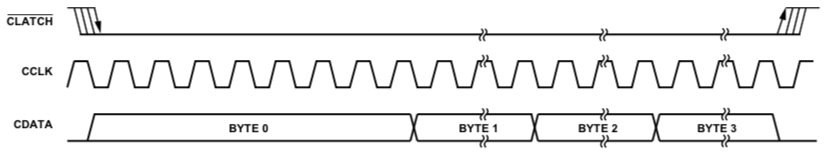 The figure to the right shows a timing diagram for a write cycle. The clock can be free running or run just during the transaction. CDATA and CLATCHn need to be setup before the rising edge of CCLK. A transaction needs at least four bytes, and the bytes are sent most significant bit first. The first byte contains seven zero bits followed by the read/write bit. The second byte contains the most significant byte of the register 16-bit address and the third byte contains the least significant byte of the address. The fourth byte is the data byte to write to the address. More than one data byte can be written and those just keep following. The address will increment by one for each subsequent byte written.
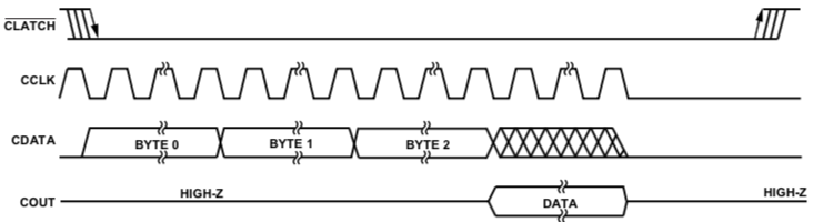 Here is an example of a read cycle. It is basically the same as the write cycle but the read/write bit is set high. The value of the CDATA input is ignored in the data part of the transaction and instead the COUT output is driven by the ADAU1761 and contains the data being read. This data is properly setup to the rising edge of the CCLK signal.
Getting Started
From Vivado, select Tools→Create and Package IP, like we have done in the other tutorials. Choose to Create a new AXI4 peripheral, and give it the name adau1761_controller. Make it an AXI4 Lite slave with six registers. Click Next and then select Edit IP and click Finish. I won’t walk through all the steps in detail as you should be familiar with them from previous tutorials, but here are the highlights.
The Big Picture
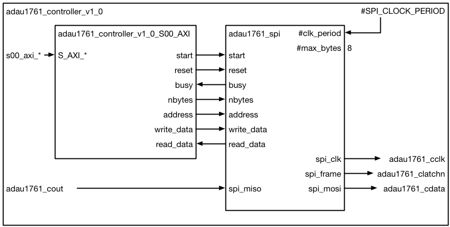
We are aiming to have an IP block which looks like the figure on the right. When we create the IP block in the IP Packager it will create the top module adau1761_controller_v1_0 and the register block adau1761_controller_v1_0_S00_AXI. We will create the adau1761_spi module and connect its control and status signals to the register block.
Modify the Register Block
Modify the adau1761_controller_v1_0_S00_AXI.v file to have the following ports. These will connect to the control and status signals in our adau1761_spi module. These allow the ARM processor to control the SPI interface and to read status from the interface.
 output wire reset,
 output wire start,
 output wire read,
 output wire [2:0] nbytes,
 output wire [15:0] address,
 output wire [63:0] write_data,
 input wire busy,
 input wire [63:0] read_data,
The reset output will reset the SPI state machine. The start output will start a SPI transaction when it rises. The read output specifies whether a read or write transaction is to occur, and the nbytes output specifies the number of bytes in a transaction. Actually it specifies one less than the number of bytes. A zero value implies one byte and a value of seven implies eight bytes. The address value is just the 16-bit address for the transaction. The write_data output specifies what data to write. Since we can write up to eight bytes of data, it is an eight byte value. However, if you send fewer than eight bytes the value needs to be justified into the most significant bytes. So for example, if you send just one byte the data needs to be in write_data[63:56].
The busy signal tells the ARM that the unit is still sending or receiving data. The read_data signal is the data that was read back from the device. The read_data value is aligned like the write_data value.
At the end of the file add the following user logic.
// Add user logic here
assign reset = slv_reg0[25];
assign start = slv_reg0[24];
assign address = slv_reg0[15:0];
assign nbytes = slv_reg0[18:16];
assign read = slv_reg0[19];
assign slv_reg1 = {{C_S_AXI_DATA_WIDTH-1{1'b0}},busy};
assign write_data[31:0] = slv_reg2;
assign write_data[63:32] = slv_reg3;
assign slv_reg4 = read_data[31:0];
assign slv_reg5 = read_data[63:32];
// User logic ends
This logic maps the register bits into the control and status wires that leave and enter the module. The control registers and readable and writeable by the ARM. These are slv_reg0, slv_reg2, and slv_reg3. We want the reset signal to come from bit 25 of slv_reg0. So the first assign makes that happen. Likewise for the other control signals. For the status signals, the assignment is the other way around. The ARM does not write to those registers but instead they are set by the status inputs to the register block. The assignment to slv_reg1 says that it’s LSB is the busy input and the other bits are always zero. Similarly the slv_reg4 and slv_reg5 and made from the read_data bits.
Register 0, 2, and 3 and readable and writeable. Registers 1, 4, and 5 are read only. You will need to change the declarations for slv_reg1, slv_reg4, and slv_reg5 to be wires and remove the logic which writes to those registers.
Controller top-level
Now let’s focus on the adau1761_controller_v1_0.v file. Add the following ports which will be used to communicate with the ADAU1761 chip.
 // Users to add ports here
 (* mark_debug = "true" *) output adau1761_cclk,
 (* mark_debug = "true" *) output adau1761_clatchn,
 (* mark_debug = "true" *) output adau1761_cdata,
 (* mark_debug = "true" *) input adau1761_cout,
Notice that we have them marked for debug. That will let us look at the interaction of the FPGA with the ADAU1761 chip later in the tutorial.
We will also need to declare the register signals which will go from our register block into our SPI controller. Here are those, also with the debug attribute.
 (* mark_debug = "true" *) wire reset;
 (* mark_debug = "true" *) wire start;
 (* mark_debug = "true" *) wire read;
 (* mark_debug = "true" *) wire [15:0] address;
 (* mark_debug = "true" *) wire [2:0] nbytes;
 (* mark_debug = "true" *) wire [63:0] write_data;
 (* mark_debug = "true" *) wire busy;
 (* mark_debug = "true" *) wire [63:0] read_data;
We added the control and status ports to the register block. Now we need to change the register block instance in the top level module to connect the wires we just defined to the new ports that we added in the previous section.
The SPI Controller
All that is left for this file is to instantiate the actual SPI controller that will do the work. We will call the module adau1761_spi and it takes two parameters. The first is called clk_period and specifies how many of our clock cycles there are in a SPI clock cycle. The assumption here is that the clock this logic is running off will be significantly faster than the SPI clock period. The maximum SPI clock period for the ADAU1761 is 100ns and we will be running off the 100MHz AXI clock. We actually probably want to run the SPI clock slower than 10MHz too, since there is no hurry and going slower is less likely to run into problems that could be difficult to debug. The second parameter is called max_bytes and it specifies the maximum number of bytes that are allowed in a SPI transaction. Because of our register layout the maximum number of bytes in this case is eight.
Actually, while we are here, let’s create a parameter for this top-level module which specifies the SPI clock period. That way a user of this IP block can specify what they want since our clock frequency may not always be 100MHz. Make the parameter called SPI_CLOCK_PERIOD.
In addition to all the control signals from the registers, our adau1761_spi block also has a clock input which is connected to the AXI clock s00_axi_aclk, and ports which connect to the ADAU1761 SPI interface. Don’t make the mistake of connecting the clk input of the adau1761_spi module to a signal called clk. There is no signal called clk at the top module. The clock at the top module is called s00_axi_aclk.
Now, as we move lower into our hierarchy of modules, we want to try to make the design more generic. This lets us reuse the design in other places. The SPI signal names at this level are all prefixed with adau1761_ and are not very generic. We will change those names in the adau1761_spi interface to have the names spi_clk, spi_frame, spi_mosi, and spi_miso. Here are the connections for that part of the instantiation.
 .spi_clk(adau1761_cclk),
 .spi_frame(adau1761_clatchn),
 .spi_mosi(adau1761_cdata),
 .spi_miso(adau1761_cout)
The clock signal is obvious, but I prefer the term frame when dealing with what the ADAU1761 calls the chip select. This is really the signal which specifies that the data on the other signals is valid and should be paid attention to. This signal frames the transaction. Also, it starts to get very confusing when you use terms like data in and data out on a SPI interface. Those terms are relative to the master or the slave. It is better to use the acronym MISO and MOSI for master out slave in and master in slave out. Those are unambiguous.
Now we are ready to tackle the SPI engine itself.
The SPI Engine
We need to first create the adau1761_spi.v file and make sure it is in the correct location in the IP repository. See my blog post on creating files in the correct location for IP packaging. If you just use the default location then Vivado will not do the right thing.
OK, let’s first declare our module and its parameters and ports.
`timescale 1ns/1ns
module adau1761_spi #
 (
 parameter clk_period = 100,
 parameter max_bytes = 8
 )
 (
 input clk,
 input reset,
 input start,
 output reg busy,
 input read,
 input [$clog2(max_bytes)-1:0] nbytes,
 input [15:0] address,
 input [max_bytes*8-1:0] write_data,
 output [max_bytes*8-1:0] read_data,
 output reg spi_clk,
 output reg spi_frame,
 output reg spi_mosi,
 input spi_miso
 );
That should be pretty self-explanatory. Next I declare a local parameter called clk_half_period. A local parameter is just a parameter which cannot be overridden by instantiating modules. They are useful to hold computed values which will not change. In this module, clk_period may be changed by the calling module but what constitutes half of that value cannot be changed by the calling module. This sounds confusing but it is not. Here is the declaration.
localparam clk_half_period = clk_period/2;
So, if the calling module says that clk_period is 100, then clk_half_period will be set to 50. If the calling module says that clk_period is 10 then clk_half_period will be 5. The calling module cannot say that clk_period is 100 and clk_half_period is 70. It can only change clk_half_period indirectly.
Next we need to watch the start signals to see if it rises. That will indicate that we need to start a SPI transaction. Doing this is a common idiom that we have seen before.
reg [1:0] start_shift = 0;
always @(posedge clk)
start_shift <= {start_shift,start};
wire start_rise = start_shift == 2'b01;
Next we keep a counter which helps us create the SPI clock. The counter starts if we are not busy and we see a rise on the start signal. It counts if we are busy, and wraps when the count is equal to the clock period minus one.
  reg [$clog2(clk_period)-1:0] clk_count;
  always @(posedge clk)
    if (reset)
      clk_count <= 0;
    else if (!busy && start_rise)
      clk_count <= 0;
    else if (busy)
      if (clk_count == clk_period-1)
	clk_count <= 0;
      else
	clk_count <= clk_count+1;
Now we look at the count values and make the SPI clock rise and fall at the correct times.
  wire clk_rise = clk_count == clk_half_period;
  wire clk_fall = clk_count == 0;
  always @(posedge clk)
    if (clk_fall) spi_clk <= 0;
    else if (clk_rise) spi_clk <= 1;
Next we need a shift register which will hold the data that we will be shifting out. This will also do double duty on read transactions and shift the read data back in.
reg [8*max_bytes+24:0] shift_reg;
We will also need a counter to count the number of bits that we have shifted so that we know when to end the transaction.
integer shift_count
Now we have an always block which will load the shift register and shift it on the falling edge of the SPI clock. Remember we need to keep the data stable around the rising edge of the clock. If you have a keen eye you will see that our shift register has one more bit than you would expect. This extra bit is used to hold the half cycle of data at the start of the transaction. Here is the always block in its entirety.
  always @(posedge clk)
    if (reset)
      busy <= 0;
    else if (!busy)
      begin
        if (start_rise)
	  begin
	    busy <= 1;
	    shift_count <= 0;
	    shift_reg <= {8'b0,read,address,write_data};
	  end
        end
    else if (clk_rise)
      shift_count <= shift_count+1;
    else if (clk_fall)
      begin
	shift_reg <= {shift_reg,spi_miso};
	if (shift_count == 32+nbytes*8)
	  busy <= 0;
      end
Basically the important parts are we reset busy when we get reset. If we are not busy when start rises, then we become busy, set our shift count to zero, and load the shift register. If we are busy and the SPI clock rises, then we increment our shift count. Otherwise if we are busy and the SPI clock falls then we shift the shift register and if we hit the total number of bytes to shift then we go back to the idle state.
One little detail. Technically we should capture the spi_miso data on the rising edge of the SPI clock. We capture it here on the falling edge right before it changes. Because the SPI clock actually falls the cycle after clk_fall is true this is safe to do.
We need to set the read_data output to the value that was shifted in to the shift register. This only needs to be stable when we are not shifting so we just pass the shift register bits back directly.
assign read_data = shift_reg[max_bytes*8-1:0];
The spi_frame output is just the inverse of busy.
always @(*) spi_frame = ~busy;
And of course the SPI output spi_mosi is just the most significant bit of the shift register.
always @(*) spi_mosi = shift_reg[8*max_bytes+24];
And don’t forget to end your module!
Now merge all the file changes and add the SPI_CLOCK_PERIOD parameter to the GUI view and package your IP.
Building the Full Chip
Now back in your original project go to the IP Integrator and instantiate an adau1761_controller IP component and the ZYNQ processor. Run all the block automations, and all the connection automations. Make the adau1761_* ports from the controller external and create the HDL wrapper by right-clicking on the audio_controller instance in the Sources window, and then run Generate Block Design.
You then need to add the constraints for the SPI interface. For expediency, here they are. You will need to modify as appropriate for the ZYBO board.
set_property IOSTANDARD LVCMOS33 [get_ports adau1761_cclk]
set_property IOSTANDARD LVCMOS33 [get_ports adau1761_clatchn]
set_property IOSTANDARD LVCMOS33 [get_ports adau1761_cdata]
set_property IOSTANDARD LVCMOS33 [get_ports adau1761_cout]
set_property PACKAGE_PIN AB4 [get_ports adau1761_cclk]
set_property PACKAGE_PIN AB1 [get_ports adau1761_clatchn]
set_property PACKAGE_PIN Y5 [get_ports adau1761_cdata]
set_property PACKAGE_PIN AB5 [get_ports adau1761_cout]
Now go ahead and Run Synthesis on the design. With that complete you should be able to Set Up Debug, found under the Flow Navigator under Synthesized Design, to add your signals that were marked for debug. This will let us watch the SPI engine talk to the ADAU1761 chip.
Ideally we would set up a simulation of the IP block using an AXI4 Lite bus functional model (BFM) and a model of the SPI interface on the ADAU1761 chip, The BFM allows the simulator to take the place of the ZYNQ processor and lets your test perform register reads and writes to stimulate the IP block. However, the BFM is a separate license from Xilinx and it is not free. I am working on a model which can be used in the IP Integrator but it is not ready yet.
After the debug core is inserted, generate a bitstream file and export it to the SDK. Then start the SDK.
The ARM Code
Once SDK starts up create a new empty application called audio_control. Add a source file main.c and start by including the xparameters and adau1761_controller header files.
#include "adau1761_controller.h"
#include "xparameters.h"
Then we define a shorter name for the base address of the controller, mnemonic names for the register offsets, and some position information for the register fields.
#define AUDIO_BASE XPAR_ADAU1761_CONTROLLER_0_S00_AXI_BASEADDR

#define CTRL_ADDR ADAU1761_CONTROLLER_S00_AXI_SLV_REG0_OFFSET
#define BUSY_ADDR ADAU1761_CONTROLLER_S00_AXI_SLV_REG1_OFFSET
#define WRITE_LOW_DATA_ADDR ADAU1761_CONTROLLER_S00_AXI_SLV_REG2_OFFSET
#define WRITE_HIGH_DATA_ADDR ADAU1761_CONTROLLER_S00_AXI_SLV_REG3_OFFSET
#define READ_LOW_DATA_ADDR ADAU1761_CONTROLLER_S00_AXI_SLV_REG4_OFFSET
#define READ_HIGH_DATA_ADDR ADAU1761_CONTROLLER_S00_AXI_SLV_REG5_OFFSET

#define RESET_POS 25
#define START_POS 24
#define READ_POS 19
#define NBYTES_POS 16
#define ADDR_POS 0
Next we define the function that will perform a write transaction. It takes as a parameter the address, the data, and the number of bytes to write. The control word is composed of one less than the number of bytes and the address value shifted into the correct positions. We don’t need to worry about the read bit because that is zero for writes. Then the low and high portions of the data value. These need to be shifted into the most significant positions. Then the registers need to be written. Note that a rising edge on the start bit is what actually kicks off the transaction and it is located in the control register. So we write the control word, and then we write the control word again with the start bit set. Then we wait until the busy register returns zero. Here is the code.
void write_adau1761(uint32_t addr, uint64_t data, uint32_t nbytes)
{
  uint32_t busy;
  uint32_t control_word = (nbytes-1)<<NBYTES_POS|
    addr<<ADDR_POS;
  uint32_t data_low = data<<(8*(8-nbytes));
  uint32_t data_high = (data<<(8*(8-nbytes)))>>32;
  ADAU1761_CONTROLLER_mWriteReg(AUDIO_BASE,WRITE_LOW_DATA_ADDR,
    data_low);
  ADAU1761_CONTROLLER_mWriteReg(AUDIO_BASE,WRITE_HIGH_DATA_ADDR,
    data_high);
  ADAU1761_CONTROLLER_mWriteReg(AUDIO_BASE,CTRL_ADDR,control_word);
  ADAU1761_CONTROLLER_mWriteReg(AUDIO_BASE,CTRL_ADDR,control_word|
    (1<<START_POS));
  while ((busy = ADAU1761_CONTROLLER_mReadReg(AUDIO_BASE,BUSY_ADDR)));
}
The read function is similar but does not take the data parameter and instead returns a 64-bit value. We again set the control word, this time with the read bit set. We write the control word and then write it again with the start bit set. We then wait for busy to be low, and then read the received data. The read data does not need to be aligned since it is shifter in to the shift register from the LSB. But it does need to be masked. Here is the read function.
uint64_t read_adau1761(uint32_t addr, uint32_t nbytes)
{
  uint32_t busy;
  uint32_t control_word = 1<<READ_POS|(nbytes-1)<<NBYTES_POS|
    addr<<ADDR_POS;
  uint64_t data_low;
  uint64_t data_high;
  ADAU1761_CONTROLLER_mWriteReg(AUDIO_BASE,CTRL_ADDR,control_word);
  ADAU1761_CONTROLLER_mWriteReg(AUDIO_BASE,CTRL_ADDR,control_word|
    (1<<START_POS));
  while ((busy = ADAU1761_CONTROLLER_mReadReg(AUDIO_BASE,BUSY_ADDR)));
  data_low = ADAU1761_CONTROLLER_mReadReg(AUDIO_BASE,
    READ_LOW_DATA_ADDR);
  data_high = ADAU1761_CONTROLLER_mReadReg(AUDIO_BASE,
    READ_HIGH_DATA_ADDR);
  return ((data_high<<32)|data_low)&((1LL<<8*nbytes)-1);
}
Next we need a function to reset the SPI controller and place the ADAU1761 chip into SPI mode. By default the chip is in I2C mode and it needs to see the CLATCH signal fall three times to switch into SPI mode. Here is the reset code.
void reset_adau1761(void)
{
  ADAU1761_CONTROLLER_mWriteReg(AUDIO_BASE,CTRL_ADDR,1<<RESET_POS);
  ADAU1761_CONTROLLER_mWriteReg(AUDIO_BASE,CTRL_ADDR,0);
  read_adau1761(0,1);
  read_adau1761(0,1);
  read_adau1761(0,1);
}
Finally we need to initialize the ADAU1761 part. This is not as easy as it sounds. There are over twenty different registers that need to be configured. There is a good tutorial on doing this written by Mike Field on his blog at ZedBoard Audio. I highly recommend giving that a read if you want to understand more about configuring the chip. You can also download the datasheet from Analog Devices and read more about the part. For the purposes of this tutorial however, we just need to write the registers with the magic values. Here’s the code.
void init_adau1761(void) {
  volatile int i;
  //  setup PLL
  write_adau1761(0x4000,0x0e,1);
  //  Configure PLL
  write_adau1761(0x4002,0x007d000c2301,6);
  //  Wait for PLL to lock
  while (!(read_adau1761(0x4002,6)&2));
  //  Enable clock to core
  write_adau1761(0x4000,0xf,1);
  //  delay
  for (i=0; i<1000000; i++);
  //  I2S master mode
  write_adau1761(0x4015,0x01,1);
  //  left mixer enable
  write_adau1761(0x400a,0x01,1);
  //  left 0db
  write_adau1761(0x400b,0x05,1);
  //  right mixer enable
  write_adau1761(0x400c,0x01,1);
  //  right 0db
  write_adau1761(0x400d,0x05,1);
  //  Playback left mixer unmute, enable
  write_adau1761(0x401c,0x21,1);
  //  Playback right mixer unmute, enable
  write_adau1761(0x401e,0x41,1);
  //  Enable headphone output left
  write_adau1761(0x4023,0xe7,1);
  //  Enable headphone output right
  write_adau1761(0x4024,0xe7,1);
  //  Enable line out left
  write_adau1761(0x4025,0xe7,1);
  //  Enable line out right
  write_adau1761(0x4026,0xe7,1);
  //  Enable both ADCs
  write_adau1761(0x4019,0x03,1);
  //  Enable playback both channels
  write_adau1761(0x4029,0x03,1);
  //  Enable both DACs
  write_adau1761(0x402a,0x03,1);
  //  Serial input L0,R0 to DAC L,R
  write_adau1761(0x40f2,0x01,1);
  //  Serial output ADC L,R to serial output L0,R0
  write_adau1761(0x40f3,0x01,1);
  //  Enable clocks to all engines
  write_adau1761(0x40f9,0x7f,1);
  //  Enable both clock generators
  write_adau1761(0x40fa,0x03,1);
}
Then you just need a main() routine to call the reset and init functions.
int main(void) {
  reset_adau1761();
  init_adau1761();
}
And there you have the C code to initialize the part. Now we will turn our attention to building the rest of the FPGA that can pass the audio through.
Generating the Audio Clock
The ADAU1761 chip needs to get a 24MHz clock from the FPGA. We will use the clocking wizard to create one for it to use. Go back to your FPGA project and open the IP Integrator. Click the Add IP icon and add a Clock Wizard component.
The Re-customize IP window should pop up. If it does not right-click on the IP component and select Re-customize IP. In the Clocking Options tab make sure the Primary clock input frequency is set to 100MHz. In the Output Clocks tab make sure the output frequency is set to 24MHz. Make sure that the Clocking Feedback source is set to Automatic Control On-Chip. Also, lower on that page make select Active Low for the Reset Type. Then click OK.
Do not run the connection automation. Connect the FCLK_CLK0 clock output from the ZYNQ to the clk_in1 input of the Clocking Wizard. Connect the FCLK_RESET0_N output from the ZYNQ to the resetn input of the Clocking Wizard. Right-click in the IP Integrator Diagram window and create an output port called adau1761_mclk and another called led0. Connect the clk_out1 port of the Clocking Wizard to the adau1761_mclk port and the locked output to the led0 port. This will let us know that the PLL has locked by looking at the LED.
Loopback the Digital Audio
Now we will construct the logic to loopback the digital audio input to the digital audio output.
The audio data coming from and going to the ADAU1761 chip uses the I2S protocol. This protocol is similar to SPI in that it uses serial data and a clock. Unlike SPI however, the data never stops. There is no concept of a transaction, it just streams constantly. Rather than a frame signal, there is a channel select signal. When the channel select signal is low the data is for the left channel and when it is high, the data is for the right channel. The data is sent most significant bit first and the data is encoded using twos complement. One device is the master and generates the serial clock and word select signal. If it is transmitting the audio data from the master to the slave, then it also sends the serial data. If it is receiving then the slave sends the serial data.
In our case, there is a transmit and receive stream of data and the ADAU1761 is the master. For all practical purposes that means we just need to take the data we receive and send it back to the master. In the next tutorial we will actually process the I2S data.
For now, create a new IP component. Give it an AXI4 Lite slave interface and eight registers. We won’t be using the registers for now. Call the IP an adau1761_data component.
To the top level module add the following ports.
   // Users to add ports here
   (* mark_debug = "true" *) input wire adau1761_bclk,
   (* mark_debug = "true" *) input wire adau1761_lrclk,
   (* mark_debug = "true" *) input wire adau1761_adc_sdata,
   (* mark_debug = "true" *) output wire adau1761_dac_sdata,
   // User ports ends
Then at the end of the file loopback the ADC data to the DAC.
  // Add user logic here
  assign adau1761_dac_sdata = adau1761_adc_sdata;
  // User logic ends
Go ahead and merge the changes and repackage the IP. Don’t worry about the registers for now. We will hook those up in the next tutorial.
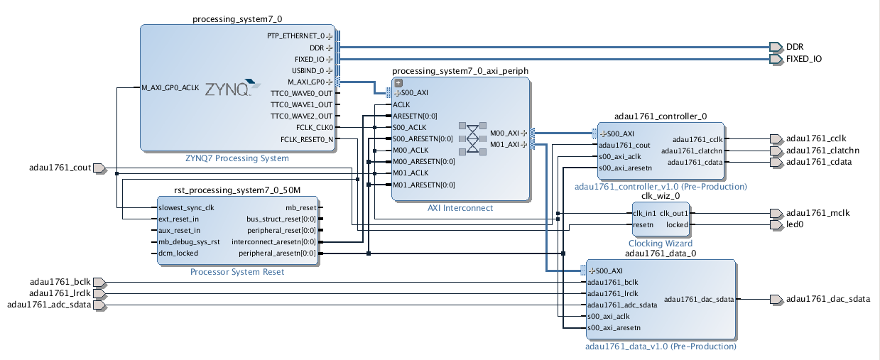 Back in your main project go ahead and run the connection automation. Then make the I2S ports external. When complete your design should look like the figure to the right. If everything looks good you should be able to generate the block design.
We need to add some pin constraints to the design as well. Here are the ones I have.
set_property IOSTANDARD LVCMOS33 [get_ports adau1761_mclk]
set_property PACKAGE_PIN AB2 [get_ports adau1761_mclk]
set_property IOSTANDARD LVCMOS33 [get_ports led0]
set_property PACKAGE_PIN T22 [get_ports led0]

set_property IOSTANDARD LVCMOS33 [get_ports adau1761_adc_sdata]
set_property IOSTANDARD LVCMOS33 [get_ports adau1761_dac_sdata]
set_property IOSTANDARD LVCMOS33 [get_ports adau1761_bclk]
set_property IOSTANDARD LVCMOS33 [get_ports adau1761_lrclk]
set_property PACKAGE_PIN AA7 [get_ports adau1761_adc_sdata]
set_property PACKAGE_PIN Y8 [get_ports adau1761_dac_sdata]
set_property PACKAGE_PIN AA6 [get_ports adau1761_bclk]
set_property PACKAGE_PIN Y6 [get_ports adau1761_lrclk]
Once the constraints are entered you should be able to synthesize the design.
Setting Up Debug
Run the Setup Debug tool to set up the embedded logic analyzer. We will use this to look at the SPI interface as well as the audio data. Since we have marked all the nets we are interested in just add all of them.Notice that some nets have an undefined clock domain. These correspond to the I2S interface signals. Also notice that there are only three signals and not four. That is because the ADC and DAC data signals are now the same. We need to define the clock domain to be used for the I2S signals. We could place them on the FCLK_CLK0 clock coming from the ZYNQ processor, but instead let’s put them on the mclk audio clock domain. This will have the effect of creating a second logic analyzer unit.
Right-clock on the red undefined label in the Clock Domain column and select Select Clock Domain… Then select the adau1761_mclk_OBUF clock. Do the same for the other undefined signals. You should then be able to clock Next. Select a sample data depth of 16384 and click Next. Then click Finish.
You should now be able to generate the bitstream.
Putting it All Together
You should be able to program the FPGA and run the program to configure the ADAU1761. Note that when you first program the FPGA you will get a message saying there are no debug cores. This is because the ARM has not yet been configured to there is no clock going to the embedded logic analyzer. Once you run the software the ARM will be configured and Vivado will be able to see the logic analyzers.
You should now be able to plug an iPod or other audio source into the line in input on the ZedBoard (the blue connector) and plug in some headphones (the black connector) and listen to your tunes. Use the embedded logic analyzer to see the digital audio as it passes through the FPGA. In the next tutorial we will actually receive the data and process it before sending it back out.
Files
Here are the files I have for this tutorial in case you get stuck or you just want to see how I implemented things.
Thanks Pete, great tutorial!
I came back to this after some time; here are some notes from the workshop of areas I had to revisit:
– In addition to “Run all block automations” I also ran “Run all connection automations” or something along those lines in the subtle turquoise on green hyperlinks at the top of the window.
– “Create HDL wrapper” is found by right-clicking on audio_controller instance in the Sources window, under Design Sources.
– The “Set up Debug” step is found under the Flow Navigator in the Synthesis section under “Synthesized Design”.
Thanks for the feedback. I have incorporated some of your comments into the tutorial. I also added some more description of what we are trying to build and a block diagram of the adau1761_controller IP. Hopefully that will be more clear to people.
Thanks Pete for the wonderful tutorial. I would like to know how to access the ADC pin AA7(adau1761_adc_sdata) from the ARM C code. This PIN is the GPIO1 pin of the ADAU1761 chip. I need to access this value from main.c. May I know how to do it? Thanks in advance.
Look at tutorial 14 to see how to make an ARM FPGA. You can make your own custom component as described in tutorial 13 or use can use a Xilinx AXI GPIO component and connect it to the pin. If you can follow and understand tutorial 13 and tutorial 14 then what you want to do should be simple.
where can I find adau1761_controller.h file
Getting error in sdk that header file in not in repository. Where can I find adau1761_controller.h file.
The adau1761_controller.h file should be in audio_controller_bsp/ps7_cortexa9_0/include.
Did you export the hardware from Vivado (check to include the bit file) and then start SDK from Vivado? This should include the audio_controller_bsp in the SDK project.
Thank you Sir.
I generated bit stream successfully and exported to SDK. Still adau1761_controller.h file is not there in adau1761_controller_bsp folder.
That’s very strange. When you create the new application in SDK it should also create the BSP. So it is creating the audio_controller_bsp for you? Does your BlockDesign look like the one in the figure in the tutorial? It is the one with the light blue boxes. Double check that you are really adding the adau1761_controller IP component. If that is in your block design then the header file should be included in your BSP.
While creating the adau1761_controller IP I used the option package current project, so I didnt get the header file.
Now I use the option create a new AXI peripheral so I find that header file in BSP folder.
Thank you very much for your response sir.
I am surprised there was no header file when you package the current project. I will have to explore that. I’m glad you got things working. The next tutorials cover doing things with the audio data so be sure to check those out.
Is it is possible to add delay to the audio samples using this design (tutorial 17) without using I2S receiver and transmitter??
Hello Sir,
Everything is working in sdk but not able to listen output from line out. Do I have to add any extra code to main.c??
You could probably do that. But tutorial 18 through 21 show you how to do that with the I2S receiver and transmitter.
You should just need the code that I have in the main.c.
If I give something in the main funtion to print on tera term it is printing. But I am not able to listen to the music. Why it is happening??
How to check whether input is successfully given through line in?? means how to print the ADC data in tera term??
Hello, sir?
It’s really good tutorial for me. But i wondering in last block diagram.
First, I completed following tutorial but the result of adau1761_controller IP different. My IP have reset, start, read, … but not yours.
Second, How can I get the adau1761_data IP?
Even I’m not able to listen to any output from headphones. I followed all the steps…Any suggestions on what might have gone wrong?
Make sure that your block design matches the one shown in the tutorial. Make sure that you are running the ARM code to configure the ADAU1761. Have you used the embedded logic analyzer to looks at the SPI signals to the ADAU1761 chip? Make sure that you are programming that correctly. Also, make sure that you are generating the 24 MHz clock to the ADAU1761. You can check that with an oscilloscope. Let me know what you find.
Hey Pete,
Thank you for your prompt reply!
1) My block design exactly matches the tutorial.
2) I program the FPGA first with the bitstream and then execute run as “Launch on hardware gdb option”
3) The embedded Logic analyser pops up after I program the device, run the software code and then click on “refresh devie”. I havent used it before. so not sure when it should pop up. Here is the catch..SPI signals show only 0’s when I click on trigger. Same is the case with audio_data signals. But bclk and lrclk is high.
4) I’m generating 24MHz clock because led0is going red indicating the signal is locked
I would have attached a snapshot if there was an option..!
You should set up the logic analyzer before running the ARM code. Set it to trigger on clatch_n falling. Otherwise you are just looking at the SPI signals when nothing is happening. Once you run the ARM code the logic analyzer should trigger and show you a waveform with something actually happening.
I am pretty sure that you have not properly configured the ADAU1761 correctly. If you did then you should be seeing the bclk and lrclk signals changing even if there is no audio data. It has been a while since I have done the tutorial so I could be wrong though.
I am also assuming that you have proper audio feeding into the device and you are using the correct line in and line out plugs.
Hi Pete,
You used Zedboard in the previous tutorials, but in this tutorial you mentioned following:
“You then need to add the constraints for the SPI interface. For expediency, here they are. You will need to modify as appropriate for the ZYBO board.” It seems to me that in this tutorial you used ZYBO board rather than the Zedboard. I am wondering If I use the zedboard, the constraint files would be the same or not.
I encountered the similar problem as Akshatha on June 8, 2016 at 9:34 am said:
Hey Pete,
Thank you for your prompt reply!
1) My block design exactly matches the tutorial.
2) I program the FPGA first with the bitstream and then execute run as “Launch on hardware gdb option”
Could you please specify more on this problem? I have already carefully each step I did in this tutorial, but I did not find anything different from yours. I spent a couple of days on this problem.
Many Thanks
Hi Pete,
I guess I could mention the parts I did that differ from the above tutorial.
Q1: In the Generating the Audio Clock part, In the Clocking Options tab make sure the Primary clock input frequency is set to 100MHz. In the Output Clocks tab make sure the output frequency is set to 24MHz. Make sure that the Clocking Feedback source is set to Automatic Control On-Chip. Also, lower on that page make select Active Low for the Reset Type. Then click OK.
I followed the steps as above except that the clock input frequency is manually set, and other settings are default.
Q2: In the Setting Up Debug part, the adau1761_mclk_OBUF clock does not exist in my design. But it have clk_out_1 in the clock domain. I used that instead.
Q3: In the Putting it All Together part, logic analyzer is set, and then run the trigger. After ARM code runs, it has same problem as Akshatha on June 8, 2016 at 9:34 am said.
BTW, how did you set up the logic analyzer? It may be the problem.
I have compared all the codes I wrote and the code you give. It’s the same. I guess it would not be the code problem.
Sorry for any inconvenience.
Alex
This tutorial is designed for the ZedBoard and not the ZYBO. I had some users that had asked about the ZYBO and the audio chip for it is different. I will change the wording so that it is more clear.
I will do the tutorial again to check everything. Are you using a newer version of Vivado? Maybe something has changed there. But if you are seeing the same thing as Akshatha then there is probably something wrong.
Thanks for bringing these things to my attention. I should be able to investigate this in the next week or so.
-Pete
Hi Pete,
I am using vivado 2015.4 64bit. As you suggested, I have checked ARM code with ADAU1761_CONTROLLER_Reg_SelfTest function to see the register is written successfully or not, and also use ILA to see the output of the 24MHz clk. These are working as expected. I guess the ILA is not triggered owing to the ADAU1761 is not appropriately configured, because as you mentioned in the previous reply, the signals of the bclk and lrclk would be changing. Additionally, the ILA would capture some signals from the ARM proessor which reset the adau1761_controller.
I will duplicate the tutorial again and see what I can get
Thanks for your reply.
Alex
Hi Pete,
Same as the stopwatch tutorial, please change the address of AXI registers as follows:
/* Definitions for peripheral ADAU1761_CONTROLLER_0 */
#define XPAR_ADAU1761_CONTROLLER_0_DEVICE_ID 0
//#define XPAR_ADAU1761_CONTROLLER_0_S00_AXI_BASEADDR 0xFFFFFFFF
//#define XPAR_ADAU1761_CONTROLLER_0_S00_AXI_HIGHADDR 0x00000000
#define XPAR_ADAU1761_CONTROLLER_0_S00_AXI_BASEADDR 0x43C00000
#define XPAR_ADAU1761_CONTROLLER_0_S00_AXI_HIGHADDR 0x43C0FFFF
/******************************************************************/
/* Definitions for driver ADAU1761_DATA */
#define XPAR_ADAU1761_DATA_NUM_INSTANCES 1
/* Definitions for peripheral ADAU1761_DATA_0 */
#define XPAR_ADAU1761_DATA_0_DEVICE_ID 0
//#define XPAR_ADAU1761_DATA_0_S00_AXI_BASEADDR 0xFFFFFFFF
//#define XPAR_ADAU1761_DATA_0_S00_AXI_HIGHADDR 0x00000000
#define XPAR_ADAU1761_DATA_0_S00_AXI_BASEADDR 0x43C10000
#define XPAR_ADAU1761_DATA_0_S00_AXI_HIGHADDR 0x43C1FFFF
Everything will be working perfectly.
AXI registers may vary with different boards, please check the address editor in the block design part, and replace these addresses with the corresponding ones.
Regards
Alex
Hi Pete,
Awesome tutorial. I have a question: why do you put nbytes-1 in the register in the SDK instead of nbytes? I can’t figure out why by myself.
Also, I suggest everybody doing this tutorial to simulate the SPI interface written by Pete on Vivado. It’s really nice to see how everything works smoothly, and also is a good exercise in writing simulation code, and you get to understand 100% the code.
Francesco,
nbytes is used by the hardware to determine how many bytes of data we want to shift out. The valid number of bytes is anywhere from 1 to 8. But if we use a four bit register we also would have 8 illegal values that someone could program. We could just use three bits and let a value of zero represent 8 bytes but this is kind of unintuitive. so I chose to have the nbytes value actually represent the number of bytes minus one. You can see in the code for shifting out the data the test for the end of shift_count
if (shift_count == 32+nbytes*8)
busy <= 0; The shift_reg value holds 8 bits of zero, the read bit, 16 bits of address and 64 bits of payload data (8 bytes). So we count from zero through 32+nbytes*8. So if you only send one byte and program nbytes to be zero then it counts from 0 through 32. Ultimately though I designed the logic to use a value of one less than the actual number of bytes - for reasons I described. And I need to make the software work accordingly. That is one of the really cool things about FPGAs. I designed it the way I wanted it to work. Both the hardware and software. Does this answer the question? Let me know if you need more in the way of explanation or if I didn't really answer your question. I'm glad you find the tutorial useful. My goal with these was to start simple but build up to something more informative. And not just tell you which buttons to press and have it all canned. You really have to work through it all to complete it. -Pete
Ok, now it’s clear. If you want to send 1 byte then shift_reg contains 8 (0s) + 1 (read) + 16 (addr) + 8 (data) = 33. So you count between 0 and 32. Which means that you have to send nbytes = 0. Cool. It was not very intuitive though 🙂 Also why you inserted the additional bit at the beginning is not intuitive at all — you need to simulate to see it. I also like the idea that you didn’t want to use 4 bits to not introduce bugs thru illegal values.
Did you omit to include these details to force us to really dig deep and simulate the code to understand it? It’s a nice strategy, I think it’s very effective and it’s the only way to really learn stuff.
It would be nice to have a tutorial covering interrupts. I believe it would really be helpful.
My intent with the tutorials was to not provide everything and have folks just nod their head that they understand. So I want people to have to figure it out and puzzle through things. Especially later in the tutorials after folks have gotten some confidence that they actually can figure things out. I have always been frustrated with vendor tutorials because they usually end up being more of a demo than a tutorial. “Look how easy our products are, you just press a button and all of these cool whizzy things can be done!”
My goal was that we would take the audio project all the way through to embedded Linux receiving audio data, processing it in some way – maybe just a delay, and then sending it back out. This would address reading and writing FPGA data and interrupts. I really have a couple more to go, but real paying work has taken most of my time. Maybe I can spend some time over the holiday break to get that working.
Thanks for the questions and feedback!
Hi Pete,
Would this SPI controller be able to pilot the MAX5216PMB1 16-bit DAC? I would like to try to pilot it w/ my own design later on just as an exercise.
Thanks.
Did you see my tutorial 24? It uses “bit banging” to basically write to that device through software. But you should also be able to write your own SPI controller in Verilog if you want to go that route or you could use the SPI device in the processor subsystem and talk to it through the Linux SPI driver.
Bit banging is the simplest if you don’t care about performance or precise timing. Writing your own SPI controller is best if you need to control the device from the FPGA and not through software or if you don’t want to deal with configuring a SPI device for Linux and use the Linux SPI driver which is complicated. The PS route is best if you want to be compatible with the Linux SPI driver.
-Pete
So my idea is to use the DAC to test the functionality of some DSP blocks that I am writing. So I need to control the DAC through the FPGA, that’s why I am asking. Is the code written for the FPGA in this Tutorial 17 reusable for any SPI interface?
Yes, you should be able to reuse it with the MAX5216. You may need to tweak a few things. The most important part is that you will need to change the design so that the data values and the start signal come from your FPGA logic rather than from an AXI register which is controlled by the ARM.
Hi Pete,
When I try to program the ARM on Eclipse, an error pops up saying “Launch failed. Binary not found”. I have tried to run with configurations but that seems to not work. Could not find the .elf file. Do you have any idea what is wrong with my application?
Baran, have you successfully compiled and run ARM code before? If so then I would double check the settings you are using. If not then maybe start with an earlier tutorial? There is probably something simple which is misconfigured. Let me know if you don’t figure it out.
-Pete
Pete,
These tutorials have been immensely helpful as I learn to program my Zybo Z7 board. I’d like to use one or more DDS Compiler blocks to directly drive PMOD DAC modules over SPI. Since the output of the DDS objects is an AXI stream, I’m wondering what the best approach is to terminating the AXI stream. (Once I do that, I’d borrow from your I2S tutorial and create the SPI signals). Should I take some other IP object (the AXI Fifo maybe?) and modify that to bridge to SPI? I’d appreciate any advice, just so that I at least start in the right direction.
Hi Pete,
I am trying to do this tutorial on Zybo Z7 board (https://reference.digilentinc.com/_media/reference/programmable-logic/zybo-z7/zybo-z7_rm.pdf) and have some trouble configuring constraints file.
I am a little bit confused is SPI possible to use on SSM2603 chip since in the datasheet there is no information about it. (http://www.analog.com/media/en/technical-documentation/data-sheets/SSM2603.pdf)
I would highly appreciate if you can help me understand and do this.
Regards,
Melisa
Mike,
Sorry for the late response. I have been traveling and just got back today.
I believe your best bet would be to write a AXI streaming to SPI module. As long as the DDS block supports flow control I don’t think you would need some type of FIFO. The DDS block would compute a new value but your SPI block won’t accept it until the old value has been transmitted. As long as the DDS can keep up, this should work. And if it can’t keep up the FIFO won’t help anyway. So, yes, modify the I2S transmit block to have it send the data out as SPI rather than I2S and you should be all set.
Let me know if you get it working or if you have more questions.
-Pete
Melisa,
The SSM2603 chip uses an I2C interface rather than a SPI interface. Don’t worry though because this is often easier to use on the Zibo than a SPI interface is. I should probably make a tutorial for using I2C devices on the ZYNQ boards. You didn’t say if you are using PetaLinux or not. If you are then you should enable an I2C core on your ZYNQ con figuration and set the interface to be EMIO. Then export the SDA and SCL pins on the block design and drive them from the top-level. The pins are bidirectional so you will see an enable pin, an input pin, and an output pin for each of the two I2C pins.
In a design where I am using I2C I have the following pins declared for the top module interface
// I2C
inout scl,
inout sda,
Then I declare wires to connect to the block design
wire iic_0_scl_i;
wire iic_0_scl_o;
wire iic_0_scl_t;
wire iic_0_sda_i;
wire iic_0_sda_o;
wire iic_0_sda_t;
Then I instantiate IO buffers usign those signals
// I2C
IOBUF scl_iobuf
(.I(iic_0_scl_o),
.IO(scl),
.O(iic_0_scl_i),
.T(iic_0_scl_t));
IOBUF sda_iobuf
(.I(iic_0_sda_o),
.IO(sda),
.O(iic_0_sda_i),
.T(iic_0_sda_t));
And then I hook those signals up to the block design instance
// I2C
.IIC_0_scl_i(iic_0_scl_i),
.IIC_0_scl_o(iic_0_scl_o),
.IIC_0_scl_t(iic_0_scl_t),
.IIC_0_sda_i(iic_0_sda_i),
.IIC_0_sda_o(iic_0_sda_o),
.IIC_0_sda_t(iic_0_sda_t),
You may need to change the port names of the block design instantiation depending on how your block design named the pins when you exported the block design.
Make sure that when you create the HDL wrapper design that you tell Vivado that you want to make edits to it.
When you export the design for Petalinux it will put the I2C device in the device tree. When you build Linux it will then have device files in /dev for the various I2C busses on the board. When you configure Petalinux be sure to turn on the I2C tools. This gives you the i2cdetect, i2cget, and is2cset tools. These can be helpful to debug I2C. You can google for how to talk to I2C devices under Linux. It is the same for all Linux so you don’t need any ZYNQ specific information on this subject.
Once you get all the I2C stuff working you still need to know how to program the SSM2603 device. There is a post about it on the Digilent forum that might help https://forum.digilentinc.com/topic/1738-how-to-use-audio-on-zybo-board/
Sorry to be so vague about this but this really requires a tutorial or blog post to cover everything. Let me know how it goes or if you have more questions.
-Pete
Pete,
Sorry for not mentioning it but I am not working with Petalinux.
So, what I understood: I have to create and package my own IP that contains bidirectional inputs, as you mentioned above? Is idea similar to SPI (making axi interface with i2c controller within like we did for SPI)?
I have enabled I2C core in Zynq PS. I followed this post, and tried to use this i2s_controller IP but I got pretty lost about idea.
I am really beginner in this and so far I didnt have problems with following your extraordinary tutorials.
I would appreciate if you can help me with this, and hopefully you will find time to cover this in future tutorials.
Regards,
Melisa
Melissa,
No problem with not using Petalinux. I think that SDK has libraries for using I2C on bare metal applications. But I have never done that before. You hook up the I2C in the FPGA like I described in my reply. But for the I2C you would use the Xilinx PS standalone driver (http://www.wiki.xilinx.com/+I2C-PS+standalone+driver). Note, you don’t want the AXI I2C driver – that’s for the I2C controller that you would instantiate in the PL.
The I2S IP in the tutorial is pretty much the same for the Zybo board. You will have an I2S input stream and output stream. You will need to find the pins that the Zybo uses for this funtion using the Zybo schematic. Look how the pins on the SSM2603 are connected to the FPGA. You will see a pad description where they connect to the FPGA usually 1 or 2 letters followed by a number. You would use those locations rather than the locations used in the tutorial for the ZedBoard.
So, to summarize. You need to connect the I2C block in the PS to the right FPGA pins. Do this as I described in my last response. Then find the I2C pins on the Zybo schematic and program the constraints for those. Likewise, find the I2S pins on the Zybo schematics and then program the constraints for those. You will need to write some custom C code using the Xilinx standalone PS I2C driver to initialize the audio codec. Look at the post I pointed to to find out more on that.
Let me know if you get stuck, and if you are successful and would like to contribute I would be happy to add what you learned to the tutorial so that others can use the Zybo board.
Thanks,
-Pete
Pete,
First of all, sorry for being so boring and thanks for your help so far.
My idea for this was to create block diagram with I2C block (for audio codec configuration) and I2S transmitter and receiver which I created with help of your tutorials. So basically what you did in tutorial 21.
Now, what is confusing me is this sentence: “You need to connect the I2C block in the PS to the right FPGA pins.” I am supposing that this Xilinx link contains C codes for initialization of the audio codec.
Can you please help me with creating my block design and then launching SDK?
P.S.
I have to mention that I found Audio Demo provided by Diligent which is not working well for me (I can not get anything from my inputs to the output): https://reference.digilentinc.com/learn/programmable-logic/tutorials/zybo-z7-dma-audio-demo/start
Melisa,
You’re not being boring at all. Let me try to clarify.
From your block design, double click on your ZYNQ Processor Subsystem. Enable the I2C interface. The important thing to know is to not add an I2C block to the block design, but rather turn on the I2C IP in the processor subsystem. If you add the I2C to the block design then the I2C will be implemented in the FPGA fabric (Programmable Logic or PL). If you enable the I2C in the ZYNQ Processor Subsystem (PS) then you are just enabling an already existing IP in the hard wired logic in the PS. There are two different library software packages, one for each type of I2C block (PS or PL). Also, when you enable the I2C subsystem in the PS you will also need to tell it to connect the pins of the IP block to the FPGA fabric (PL). The I2C pins will become visible on the PS component in the block design. Right click on the I2C interface in the block design and say to make the pin external. This connect the pins on the I2C interface to the ports on the block design.
You should probably have Vivado create a new HDL wrapper this time. But tell it you want to be able to modify the wrapper. If you have already done this step you may have to delete the wrapper and start over. The important thing to remember about the interface is that the I2C pins are bidirectional. They can be both inputs and outputs. While this is allowed on the pins of the FPGA, there is no concept internally to the fabric about bidirectional signals. Therefore there will be three signals coming in and out of the block design for each I2C pin. One is the input value from the I2C pin going in to the block design. The other two are outputs which say what value to drive out on the bidirectional pin and whether the bidirectional pin is an input or output at any moment. These three signals called iic_0_sda_o (SDA output value), iic_0_sda_t (SDA direction or “tristate” value), and iic_0_sda_i (SDA input value) are connected to an IOBUF (bidirectional input/output buffer) along with the sda pin which is the external signal. Likewise for the scl pin. The sda and scl pins are the external FPGA pins for I2C and you need to specify a location constraint for these signals. This is similar to what you do for the I2S interface signals.
After you compile the design and make a bit file you will need to export the design to SDK. From there you should be able to use the Xilinx package I linked to for the I2C PS standalone driver to talk to the codec.
In general a lot of this stuff is covered in earlier tutorials so be sure you understand the steps described in those.
Let me know if you have more questions.
-Pete
Thanks Pete! That makes sense, and I’ll proceed accordingly.
Pete,
I have followed the tutorial and built a project on PYNQ-Z2 fpga board. I loopback ADC data to DAC data and clearly hear the music played on my computer.
However, how to deal with noise? I can here the high frequency noise when I plug my PC into line-in input.
I have tried noise-gate function provided by adau1761 but I just get poor result.
English is not my mother tongue, please excuse any errors on my part.
Rick,
I haven’t used the PYNQ-Z2 board. Maybe it’s a board problem. Are there any other reference designs for the board which use audio? Do those also have a noise issue? Does the noise change if you wiggle the audio cable? Is the noise analog in nature or do you think it is digital? Maybe some of the data bits are not connected in the right order? I would double check your IO mappings. I don’t have a PYNQ-Z2 board but I do have a PYNQ-Z1. Are they compatible?
Your English is excellent by the way.
-Pete
Pete,
I didn’t find any other reference design for PYNQ-Z2 board. Most of the open source design are based on Zedboard. I am not sure if Z1 is compatible with Z2 because this is
the first time I use Xilinx FPGA board. Actually the noise is not a big issue because it can only be heard when the music is stopped. I think the noise is digital and it was changed when I wiggle the PC-to-Line-In cable.
By the way, I want to do frequency analysis to the audio signal in my project. (ref:https://github.com/filipamator/vu_meter) I care about noise issue because it might affect the result. However, the frequency of noise is in some band in frequency domain. So I think I can just ignore specific data after FFT. Or maybe the filter ip in Vivado is helpful.
Thanks for your reply.
I’m working on a zedboard fpga project which actually take input from the keyboard and uses it to produce the sound e.g. if I press ‘A’ then the sound A come from the fpga .It uses the audio codec and keyboard. I have absolutely no idea how to interface them with the zedboard and also I want to store the audio in the fpga which will be the output from Audio codec of Zedboard.
Kindly Provide some ideas or resource in order to accomplish this, if possible.
Thanks,
I have some questions about what you are trying to do. What do you mean by “keyboard”? Just a terminal attached to a UART? Or some other hardware connected to the board? If you use Petalinux then you can store the audio files on the same SD card which holds Linux. You can have a Linux app which reads from the terminal connected to the serial UART and then plays the audio samples. You could use an AXI FIFO and have the ARM write audio samples into the FIFO and then use the I2S IP or the IP used in my tutorial to send the samples to the CODEC.
Does this help?