
In this tutorial we will build an IP component that can be used by the ARM processor to implement the stopwatch ourunctions we used in our earlier tutorials. The main components of this IP block will be:
- A set of registers controlled by the ARM which control the value shown on the LEDs or the SSD
- A set of registers that the ARM reads, which read the value of the encoder register, the button and switch inputs, and a timer value maintained by the FPGA logic.
- The encoder block from tutorial 12
- The debounce logic from tutorial 11
- The seven segment display controller from tutorial 5
- A millisecond counter which the ARM uses to measure the passage of time
Creating the project
 Launch Vivado
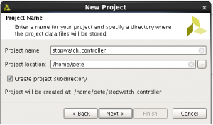
- Select Create New Project from the Getting Started screen.
 The New Project box will open. Click Next.
- Create a new project called stopwatch_controller. Click Next.
- Select RTL Project for the Project Type and click Next.
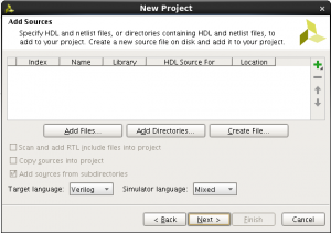
- In the Add Sources select Verilog as the Target Language, and clock Next.
- The Add Existing IP (optional) dialog opens. We have no existing IP, so click Next.
 The Add Constraints (optional) dialog opens. We will add our constraints later, so click Next.
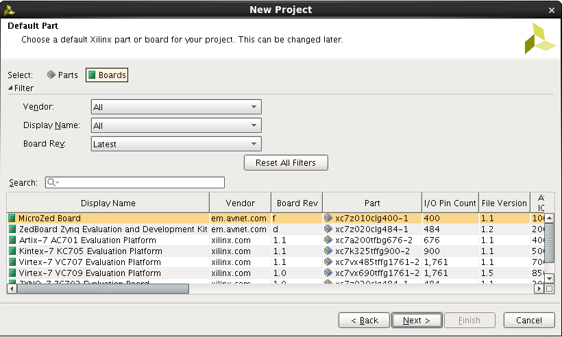
- When the Default Part dialog opens, select Boards and then select the ZedBoard option and clock Next.
- Click Finish in the New Project Summary dialog to finish creating the project.

Create the IP Block
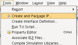 From the Tools menu, select Create and Package IP. This launches the Create and Package IP Wizard. We will use this wizard to create an IP block so that the ARM can control the seven segment display, the LEDs and switches, and the rotary encoder.
- Click Next in response to the Create and Package IP dialog.
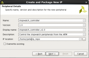 Select that we want to Create a new AXI4 peripheral in the Choose Create Peripheral or Package IP dialog. Then click Next.
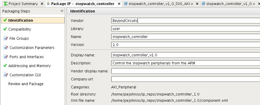
- Fill out the Peripheral Details dialog according to the figure. This gives users some identifying information when the use the IP block. Click Next.
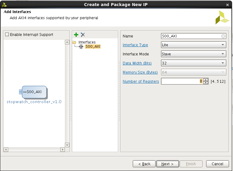
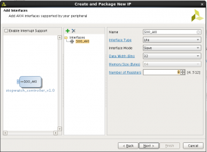 The Add Interfaces dialog box lets us setup the interface between the ARM and our IP block. We want an AXI-Lite interface with eight registers. We also want a 32-bit Slave interface. Leave the Name field as the default. When finished click Next.
- In the Create Peripheral dialog select the Edit IP option and then click Finish. A new Vivado project called edit_stopwatch_controller_v1_0 will be created.

It is important to note that this is a new project, not the one we created at the beginning of this tutorial. This new project exists while we are creating or editing our IP block, but when we complete the IP block, it will be packaged and stored in our IP repository, and this project will be deleted. If you need to edit or modify the IP block, you need to follow the steps provided later in this tutorial.
Editing the Verilog
Two source files have been created. These are:
- stopwatch_controller_v1_0 — This file instantiates the AXI-Lite interface.
- stopwatch_controller_v1_0_S00_AXI — This file contains the AXI-Lite bus functionality. As it is now, this file just implements four 32-bit registers with an AXI-Lite interface.
We need to be able to control a number of output values, as well as to write to an 8-bit value to drive on the seven segment display. We also need an 8-bit value to drive the eight LED outputs. Further, we’ll need need to be able to read an 8-bit register which holds the value of the rotary encoder and the value of the input switches and buttons. We will use the following address mapping:
| Address | Register |
|---|---|
| 0 | SSD output |
| 1 | LED output |
| 2 | switches |
| 3 | buttons |
| 4 | rotary encoder value |
| 5 | rotary encoder switch |
| 6 | rotary encoder shaft button |
| 7 | timer |
The SSD output register will just cause whatever is written to that register to display on the seven segment display. Likewise, the LED output register will cause the eight bits written to that register to appear on the eight LEDs.
The ARM will read the values of the switches from an 8-bit register at address 2, and the value of the buttons from a 5-bit register at address 3.
For the rotary encoder, we will manage the rotary pulses in hardware on the FPGA. We will keep an 8-bit register and increment or decrement it as appropriate based on the enc_a and enc_b inputs. The ARM will be able to read the value of this register at address 4. The single bit value for the rotary encoder switch and shaft button will be read at addresses 5 and 6 respectively.
Finally, we will make a special 32-bit counter which increments once per millisecond at address 7. This will be used by the software to control timing.
When the Create and Package IP Wizard ran it created a Verilog module called stopwatch_controller_v1_0_S00_AXI which implements eight 32-bit registers that can be written and read by the ARM. If you look at the Verilog code you will find that the registers inside the module are called slv_reg0 through slv_reg7. Please keep in mind that we will be discussing two entirely different things called registers. The first is flip-flop elements used throughout our Verilog code that are declared with the reg keyword. The second type are values which can be written and read by the ARM. Confusingly, sometimes these second type of registers are declared using the Verilog wire keyword and they aren’t registers at all in the Verilog sense. After a while this won’t be as confusing as you might think.
Anyway, if you look at our register list above, only the first two can be written by the ARM. It doesn’t do us any good to keep them hidden away in the stopwatch_controller_v1_0_S00_AXI module, so we will bring them out as outputs of the module. Just declare them as output reg values (in the Verilog sense) of the module.
In the Verilog code you will find eight lines that declare the slv_reg0 through slv_reg7 variables. Go ahead and cut them out and paste them in the port declaration part of the module right below the comment <code>// Users to add ports here</code>. Declare slv_reg0 and slv_reg1 to be reg outputs. Don’t forget to change the semicolon at the end of the line to a comma! These two registers (ARM sense) are outputs of the stopwatch_controller_v1_0_S00_AXI module because it is the ARM which controls their value. The other registers are inputs to the module because their value is controlled by the FPGA. The value of those registers can only be read by the ARM. Go ahead and declare them as module inputs now. Here is what my code looks like now:
		// Users to add ports here
    	output reg [C_S_AXI_DATA_WIDTH-1:0] slv_reg0,
        output reg [C_S_AXI_DATA_WIDTH-1:0] slv_reg1,
        input wire [C_S_AXI_DATA_WIDTH-1:0] slv_reg2,
        input wire [C_S_AXI_DATA_WIDTH-1:0] slv_reg3,
        input wire [C_S_AXI_DATA_WIDTH-1:0] slv_reg4,
        input wire [C_S_AXI_DATA_WIDTH-1:0] slv_reg5,
        input wire [C_S_AXI_DATA_WIDTH-1:0] slv_reg6,
        input wire [C_S_AXI_DATA_WIDTH-1:0] slv_reg7,
Now, we need to remove all the code in the module which writes to registers slv_reg2 through slv_reg7. Remember, the ARM does not get to control those values. Search down in your text editor for slv_reg2. Delete any references you see to assigning to these registers. In the end, you should only see references to these register values in the port declaration and in the case statement where the module drives the data back to the ARM. Go ahead and save your module.
Adding the logic
Now go ahead and edit the stopwatch_controller_v1_0 module. Notice that the module instantiates the stopwatch_controller_v1_0_S00_AXI module. We added eight ports to that module so we should go ahead and add them to the instantiation of the module as well. We’ll just leave them unconnected for now. My code for that looks like this:
// Instantiation of Axi Bus Interface S00_AXI
	stopwatch_controller_v1_0_S00_AXI # (
		.C_S_AXI_DATA_WIDTH(C_S00_AXI_DATA_WIDTH),
		.C_S_AXI_ADDR_WIDTH(C_S00_AXI_ADDR_WIDTH)
	) stopwatch_controller_v1_0_S00_AXI_inst (
	    .slv_reg0(),
	    .slv_reg1(),
	    .slv_reg2(),
	    .slv_reg3(),
	    .slv_reg4(),
	    .slv_reg5(),
	    .slv_reg6(),
	    .slv_reg7(),
	    .S_AXI_ACLK(s00_axi_aclk),
Next, we need to add the ports to this module. In our final design, these new ports will connect up with the outside world. We declare ports for the SSD and SSD cathode signals, the switches, the buttons, the LEDs, and the signals for the rotary encoder. Do this right below the comment which reads // Users to add ports here. Here is what I have:
		// Users to add ports here
                input wire clk,
		output wire [6:0] ssd,
		output wire ssdcat,
		output wire [7:0] led,
		input wire [4:0] btn,
		input wire [7:0] switch,
		input wire enc_a,
		input wire enc_b,
		input wire enc_sw,
		input wire enc_btn,
		// User ports ends
OK, now the real work begins. The easiest thing is the LED values. Those come directly from the ARM register slv_reg1. We just need to hook that output from the register module to the LEDs. The only gotcha is that the register is 32 bits and we only need eight. We can just wire up the led output to the slv_reg1 output of the register module, but that will give us some warnings that the widths don’t match. To keep things clean, we will connect up a 32-bit value that comes from concatenating a 24-bit Z value with our 8-bit led output. It’s important to note that we can’t use zero values here, because we would then be driving those into the register module. Here is the modification to the instantiation of the register module:
.slv_reg1({24'bz,led}),Next, let’s deal with the SSD value. Remember, what is coming out of the register module is an 8-bit value which we want to display on the seven segment display. Specifically, this is not the value of the ssd output. We will need to declare a new 8-bit wire to hold this value in our module. Let’s call that ssd_value. We need to declare that before we instantiate the register module.
wire [7:0] ssd_value;Then we need to connect that to the slv_reg0 output of the register module. Here is that modified connection:
.slv_reg0({24'bz,ssd_value}),We need to debounce all of the button and switch inputs. We will need signals to hold the debounced versions of those inputs so go ahead and declare those now. This is just like in the previous tutorial. Put these declarations right after the ssd_value declaration. Here is what I have:
	wire [7:0] switch_db;
	wire [4:0] btn_db;
	wire enc_a_db;
	wire enc_b_db;
	wire enc_sw_db;
	wire enc_btn_db;
Now some of these just go straight into the register module. Let’s put those in now. As with the first two register values, we have some width mismatches. We will use a concatenation here as well, but since we are driving inputs into the module, we’re going to need to give them an actual value. We will use zero for that. Here are the modified register module ports:
	    .slv_reg0({24'bz,ssd_value}),
	    .slv_reg1({24'bz,led}),
	    .slv_reg2({24'b0,switch_db}),
	    .slv_reg3({27'b0,btn_db}),
	    .slv_reg4(),
	    .slv_reg5({31'b0,enc_sw_db}),
	    .slv_reg6({31'b0,enc_btn_db}),
	    .slv_reg7(),
Notice that we still have to declare the 8-bit register which holds the rotary encoder value and the 32-bit timer value. Add the declarations for those before the register module instantiation like this:
	wire [7:0] encoder_value;
	reg [31:0] timer = 0;
And add those to the register module instantiation as well:
	    .slv_reg0({24'bz,ssd_value}),
	    .slv_reg1({24'bz,led}),
	    .slv_reg2({24'b0,switch_db}),
	    .slv_reg3({27'b0,btn_db}),
	    .slv_reg4({24'b0,encoder_value}),
	    .slv_reg5({31'b0,enc_sw_db}),
	    .slv_reg6({31'b0,enc_btn_db}),
	    .slv_reg7(timer),
Now is probably a good time to check that the code you have so far compiles correctly. You can click on the Elaborated Design flow under the RTL Analysis section of the Flow Navigator window. This will check your design for errors. When you are done, you can click on the Project Manager flow to get back to editing your design.
Debounce
Next, we will instantiate the debounce module from tutorial 11. We don’t need to bother with connecting the rising edge or falling edge outputs. We just need the debounced outputs. In case you are worried that this is inefficient, the synthesis tools will take care of removing any logic which does not produce an output. So rest assured: anything that is unused will not occupy space on the device.
Instantiate the debounce module like this. Note that this module does not have the ms_limit parameter so we just use a literal value of 300,000. Your code should go at the end of the module where the comments in the module indicate.
    debounce
    #(
      .width(17),
      .bounce_limit(300000)
      )
    debounce
    (
     .clk(clk),
     .switch_in({enc_a,enc_b,enc_sw,enc_btn,
		 btn,switch}),
     .switch_out({enc_a_db,enc_b_db,enc_sw_db,enc_btn_db,
		  btn_db,switch_db}),
     .switch_rise(),
     .switch_fall()
     );
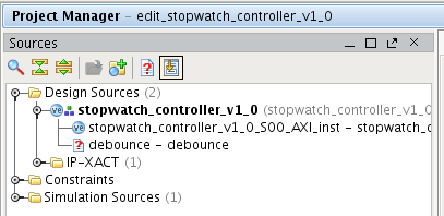 Save the code and look in the Sources window in the Project Manager flow. You will see that we have an undefined module called debounce.
We need to add the debounce module from tutorial 11 to our design. Click the Add Sources button or type ctrl-A to add a source file. Select Add or create design sources and click Next. Click Add Files… and browse to your debounce module. Check the box that says Copy sources into IP Directory. Then click Finish. You should then see the debounce module properly defined in the Sources window.
Click on the RTL Analysis flow. At the top of the Elaborated Design window, you should see an indication that the design sources have been modified. Click the Reload button to recheck your code. It will build a little block diagram of your design so far. You should see the debounce module connected to the stopwatch_controller_v1_0_S00_AXI module. Go back to the Project Manager flow.
SSD control
We also need to add the logic to control the seven segment display. This is just like in tutorial 12, except the name of the signal connected to the value input is different and we don’t have the ms_limit parameter.
  ssd
    #(100000)
  ssd
    (
     .clk(clk),
     .value(ssd_value),
     .ssd(ssd),
     .ssdcat(ssdcat)
     );
Go ahead and add the ssd module to the design using the Add Sources button. Elaborate the design again to check your RTL.
Rotary Encoder
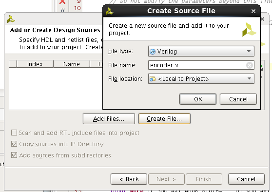 Now we need to add the logic from the rotary encoder. Let’s go ahead and put that in a module of its own and instantiate that in our top level. Add another source file, but this time, select Create File in the Add or Create Design Sources dialog box. Enter the name
 encoder.v for the file name. You cannot use the default location however. See my blog post on the subject for more details. In File location, navigate to the stopwatch_controller_v1_0 directory in the ip_repo directory and then select the hdl directory. This will place the new file in the correct location so that it is picked up by the IP packager. Click OK, and then click Finish. It will then bring up the Define Module dialog box. Just click OK until the dialog boxes go away. If you think it’s easier to declare module ports with the dialog box than typing the Verilog code, you might want to go back to tutorial 1. Or maybe you are just used to coding in VHDL.
Edit the encoder.v file and add your code from tutorial 12. Make sure to add the input and output port declarations as well. I have changed the names around a little and added a parameter to let a user specify an arbitrary width for the register. Here is my code:
`timescale 1ns / 1ns
module encoder
 #(
     parameter width = 8
  )
  (
    input clk,
    input a_rise,
    input b_value,
    output reg [width-1:0] value
  );
    initial value = 0;
    always @(posedge clk)
      if (a_rise)
        if (!b_value)
      value <= value-1;
        else
      value <= value+1;

endmodule
We also need to instantiate the encoder module. However, we’ve forgotten something. The encoder module needs to see the rise signal on the enc_a input. We can either modify the encoder module to detect the rise on the encoder input, or we can connect the a signal between the appropriate rise output of the debounce module and the encoder module. In general, it is best to keep the interface to modules as simple as possible, and I think the correct decision is to put the logic inside the encoder module. Speaking of keeping things generalized, we should probably remove the requirement that the inputs be synchronized to the module’s clock. In our case they are, but they might not be in other cases where the encoder module is used. One other minor quibble: you may have noticed that in tutorial 12 the display always started at a value of 01. That’s because the idle state of the A input from the encoder is actually high, yet we were initializing the rise detector circuit with all zeroes. That made the rise get detected when the FPGA first started up. We could initialize the rise detector here to all ones and that would not happen. But is that the case for all rotary encoders? We should probably make that a parameter as well. So let’s make a little change to that. Here is the modified module:
`timescale 1ns / 1ns
module encoder
 #(
     parameter width = 8,
     parameter a_rest_state = 1
  )
  (
    input clk,
    input a_value,
    input b_value,
    output reg [width-1:0] value
  );
    reg [1:0] a_shift = {2 {a_rest_state[0]}};
    always @(posedge clk) a_shift <= {a_shift,a_value};
    initial value = 0;
    always @(posedge clk)
      if (a_shift == 2'b01)
        if (!b_value)
      value <= value-1;
        else
      value <= value+1;
endmodule
Let’s take a little closer look at where we declare a_shift. The initialization value has two interesting features. The first is a repeated concatenation. The expression {2 {a_rest_state[0]}} means that the value in the inner curly braces is to be repeated the number of times mentioned in the outer braces. So in other words the expression {2 {value}} equivalent to {value,value}. The expression {4 {value}} is equivalent to the expression {value,value,value,value}. The other thing to note is that we are only concerned with the least significant bit of the a_rest_state parameter. It is critical that we only concatenate the 1-bit value. If we were to not do the bit select in the concatenation we would end up concatenating a 32-bit expression. This would result in a 64-bit expression and we would use the low two bits, causing a_shift to initialize to the value 2’b01 rather than the desired value of 2’b11.
Now that we have perfected our encoder module, we turn our attention to instantiating it in the top module. Here is the code I have for that:
    encoder
       #(8,1)
    encoder
       (
        .clk(clk),
        .a_value(enc_a_db),
        .b_value(enc_b_db),
        .value(encoder_value)
        );
The timer register
All that’s left is to implement the timer counter. Basically, we just want a 32-bit register which increments once every millisecond. This means we also need to have a counter to count the milliseconds as well. In thinking about this, it seems like we should probably add a ms_limit parameter to our design as well so a user of the IP block could use a clock of arbitrary frequency. Let’s go ahead and add that now. First add the parameter to the stopwatch_controller_v1_0 module. Set the default value to 100000.
// Users to add parameters here
parameter ms_limit = 100000,
// User parameters ends
We also need to modify the instantiations of debounce and ssd to use the ms_limit parameter. Remember, we used a value based on ms_limit for the debounce module. So we’ll need to turn that back into an expression based on ms_limit.
Let’s code the timer now. First, we need the millisecond counter. You should be familiar with doing this from previous tutorials. Here is the code that I have:
        reg [$clog2(ms_limit)-1:0] ms_counter = 0;
        wire ms_limit_reached = ms_counter == ms_limit-1;
        always @(posedge clk)
            if (ms_limit_reached)
                ms_counter <= 0;
            else
                ms_counter <= ms_counter+1;

        always @(posedge clk)
            if (ms_limit_reached)
                timer <= timer+1;
You can go ahead and check the code by elaborating, and you can even run a synthesis to make sure everything is OK.
Packaging the IP
 Next we turn to packaging the IP component. In the Project Manager flow, you will see a tab labeled Package IP – stopwatch_controller.
 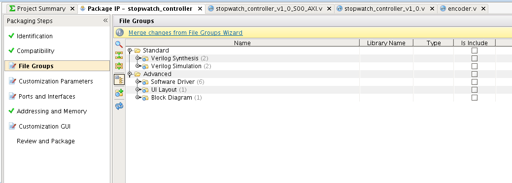 Click on the tab now. You will see a number of Packaging Steps. Some of these are checked indicating that they are complete, while others need to be updated. Go ahead and click on File Groups. You will see something like the figure to the right. Go ahead and click the link that says Merge Changes from File Groups Wizard.
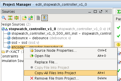 I noticed that when I ran the merge that there were warnings about the encoder.v file not having a relative path to the IP root directory. I’m not sure why I got that message– maybe it was because we created the file, rather than importing it. In any case, select the file in the Sources window and right click and select Copy All Files Into Project.
Now go to the Customization Parameters step and run the link for that step as well. Notice that this has now included the ms_limit parameter into the Customization Parameters. After this, select the Customization GUI step which allows to change what a user sees when they try to customize the IP block. You need to click on the plus icon on the Layout panel to add the ms_limit parameter. You can drag the parameter around in the Layout panel to make the parameter appear on the same page as the four existing AXI parameters.
Go to the Review and Package flow and click the link edit package settings. Make sure the option Create archive of IP is checked. Click OK. Then click Re-Package IP. Click OK to close the project.
You will now be placed back in the project we created at the beginning of this tutorial.
Packaging
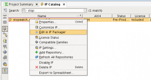 A key concept is the idea of an IP package and an IP repository. When you package your IP, Vivado places it in the IP repository. If you want to edit the IP open the IP Catalog from the Project Manager flow. Then select your IP component from the IP Catalog tab. Right click on your component and select Edit in IP Packager. This will reopen the package and edit in the appropriate context. You can then repackage the IP when you have finished your edits.
Summary
We have successfully created an IP block that we can use in the next tutorial to talk with the ARM processor. When the Package IP process completes you will be back in the project you originally created. This is where we will start our next tutorial.
Files
Here are the files I have for this tutorial.
Why are we selecting the MicroZed board for this tutorial instead of the ZedZynq board that we selected previously?
My mistake. It’s a typo. Select ZedBoard.
I do not see a tab labeled Package IP – stopwatch_controller. under the Project Manager Flow of the UI
From goggling it – From the Tools menu, select the Create and Package IP command to open the Create and Package 1.IP Wizard.
The Welcome window opens for the Create And Package New IP dialog box.
That means you are not editing an IP design. You need to be sure you have opened the project using the Create and Package IP command.
These four registers make up the four registers in the address space of our IP block. We will use the following address mapping.
I suppose it would be eight registers used for AXI Lite interface. Am I wrong?
It is eight registers. The text was wrong. I removed the sentence that was causing confusion. Let me know how the tutorial is working for you.
Hi Pete,
I haven’t complete the tutorial yet, I am still waiting for my rotary encoder delivery. I will let you know if I complete this tutorial.
Additionally, I jumped to tutorial 17 which can be completed without rotary encoder. But I read through the tutorials just in case.