GPIO with ZYNQ and PetaLinux

Accessing GPIO controllers is pretty straightforward with PetaLinux, but there are a few tricks you need to know.

Locating the GPIO controller

In the example FPGA I am using, there are two GPIO controllers in the programmable logic. These are at address 0x4120_0000 and 0x4121_0000. If you look in the pl.dtsi file in your PetaLinux project, in the directory subsystems/linux/configs/device-tree, you will see entries for the GPIO devices. There’s no need to modify the entire device tree.

If you make a PetaLinux build and boot it, you can look in the /sys/class/gpio directory.

root@pz-7015-2016-2:~# ls /sys/class/gpio/                       
export       gpiochip901  gpiochip902  gpiochip906  unexport

You can see that there is a gpiochip directory for each GPIO controller. The gpiochip901 and gpiochip902 directories correspond to the PL controllers that I added in my design. The gpiochip906 directory is for the GPIO controller in the PS.

How will you know which is which, though? Each directory contains a label file which tells you the device tree label for the controller. You can go ahead and look at the contents:

root@pz-7015-2016-2:~# cat /sys/class/gpio/gpiochip901/label 
/amba_pl/gpio@41210000
root@pz-7015-2016-2:~# cat /sys/class/gpio/gpiochip902/label 
/amba_pl/gpio@41200000
root@pz-7015-2016-2:~# cat /sys/class/gpio/gpiochip906/label 
zynq_gpio

Looking at it, you’ll see that gpiochip901 corresponds to my controller at 0x4120_0000 and gpiochip902 corresponds to the controller at 0x4121_0000. Gpiochip906 is different, and corresponds to the built-in controller on the ZYNQ. Why those numbers? In my FPGA, the first GPIO controller controls only a single GPIO bit, while the second controls four bits. We can tell how many bits each controller controls by looking in the ngpio file for the controller.

root@pz-7015-2016-2:~# cat /sys/class/gpio/gpiochip901/ngpio 
1
root@pz-7015-2016-2:~# cat /sys/class/gpio/gpiochip902/ngpio
4
root@pz-7015-2016-2:~# cat /sys/class/gpio/gpiochip906/ngpio
118

It looks to me like the numbering starts at 901. Since that controller has only a single GPIO bit, the next controller is 902. That one has four bits, so the ZYNQ PS controller goes at 906, which has 118 bits.

Enabling the GPIO bits

To access a GPIO bit, you need to enable the correct GPIO pin. You do that by writing to the export file in the /sys/class/gpio directory. Here is an example of enabling the LSB of my second controller:

root@pz-7015-2016-2:~# echo -n 902 > /sys/class/gpio/export 

Now if you look in the /sys/class/gpio directory, you will see a new directory created which allows you to control the individual GPIO pin.

root@pz-7015-2016-2:~# ls /sys/class/gpio
export       gpio902      gpiochip901  gpiochip902  gpiochip906  unexport

If you look in that directory you see a number of controls:

root@pz-7015-2016-2:~# ls /sys/class/gpio/gpio902
active_low  direction   power       subsystem   uevent      value

Accessing the GPIO bits

You can determine the GPIO direction by looking at the direction file. Since my GPIO pin is an output, it gives the value out.

root@pz-7015-2016-2:~# cat /sys/class/gpio/gpio902/direction
out

You can change the value to a 1 by writing to the value file.

root@pz-7015-2016-2:~# echo 1 > /sys/class/gpio/gpio902/value           

Conclusion

So there you have it. The “official” way to access GPIO on PetaLinux.

SPI with PetaLinux on ZYNQ

Recently, I spent a lot of time trying to get SPI working on a PicoZed ZYNQ board under Linux. It was absolutely shocking how complicated this ended up being. One issue, I think, is that the device tree options differ depending on which version of PetaLinux you’re using. In this post, I’m going to document here how to do it with PetaLinux 2016.2.

Modify the device tree

First, you need to modify the system-top.dts file located in your PetaLinux project’s subsystems/linux/configs/device-tree directory. You need to add an entry that extends the existing entry for the SPI device. In the example, I am using spi0 on the processor subsystem. You can see the base definition for the SPI interface in the zynq-7000.dtsi include file in the same directory.

It’s important to note that PetaLinux will create an entry for the SPI device when you configure Linux– however, you won’t get a device file unless you add the entry for your particular SPI device. The trick is to add the SPI device information to the file system-top.dts. The device tree specification syntax allows you to make changes to the automatic entry for the SPI device by labeling a a node, then overlaying additional information onto the labeled node in other parts of the device tree specification.

In our case, the processor built-in SPI devices are labeled spi0 and spi1. I wanted to use spi0, so I added an entry in the system-top.dts file to add to the spi0 definition. In the example below, I’ve added three devices.

&spi0 {
  is-decoded-cs = <0>;
  num-cs = <3>;
  status = "okay";
  spidev@0x00 {
    compatible = "spidev";
    spi-max-frequency = <1000000>;
    reg = <0>;
  };
  spidev@0x01 {
    compatible = "spidev";
    spi-max-frequency = <1000000>;
    reg = <1>;
  };
  spidev@0x02 {
    compatible = "spidev";
    spi-max-frequency = <1000000>;
    reg = <2>;
  };
};

Rebuild linux and reboot your PicoZed board and you can now see the device files.

root@pz-7015-2016-2:~# ls -l /dev/spi*
crw-rw----    1 root     root      153,   0 Jan  1 00:00 /dev/spidev32766.0
crw-rw----    1 root     root      153,   1 Jan  1 00:00 /dev/spidev32766.1
crw-rw----    1 root     root      153,   2 Jan  1 00:00 /dev/spidev32766.2

Testing the SPI interface

In order to test the SPI interface, I built an FPGA with the SPI ports marked for debug. This allows me to use the embedded logic analyzer to view the pin activity from Vivado. PetaLinux ships with a program to test the SPI interface called spidev_test. I compiled it with the following command:

arm-xilinx-linux-gnueabi-gcc -o spidev_test /tools/xilinx/petalinux-v2016.2-final/components/linux-kernel/xlnx-4.4/Documentation/spi/spidev_test.c

Then, I copied it to my board using ssh, configured the logic analyzer to capture SPI activity, and ran the following command:

root@pz-7015-2016-2:~# ./spidev_test -D /dev/spidev32766.0 --speed 10000000
spi mode: 0x0
bits per word: 8
max speed: 10000000 Hz (10000 KHz)
RX | 00 00 00 00 00 00 00 00 00 00 00 00 00 00 00 00 00 00 00 00 00 00 00 00 00 00 00 00 00 00 00 00  | ................................

I could see the SPI pins wiggle in the logic analyzer view.

Conclusion

Anyway, I hope that this you save some time getting SPI to work.

PetaLinux for the PicoZed

I recently ran into a SNAFU when trying to build a PetaLinux image for a PicoZed board on a rev 2 FMC carrier board. The instructions assume that you have built an FPGA image and exported it from Vivado. You can check out my tutorial on PetaLinux for more background information, just in case you’re unfamiliar with the process.

You’re going to need to make sure that you have the board support package for the PicoZed board and carrier board you are using, which can download here. I like to keep the BSP in my Xilinx tool area, but you can store it anywhere you like. Be sure to unzip the download file.

Create the project

First, I source the settings file for PetaLinux. Don’t worry about the tftp warnings.

% . /tools/xilinx/petalinux-v2015.4-final/settings.sh

Now create your PetaLinux project. I created it as a sibling of the Vivado project directory.

% petalinux-create --type project --name pz_linux --source /tools/xilinx/pz_7015_2015_4.bsp

Configure the project

Next, you configure the project with the FPGA export. This sets the device tree for the build:

% petalinux-config --get-hw-description my_fpga/my_fpga.sdk --project pz_linux

Then, configure your filesystem:

% petalinux-config -c rootfs --project pz_linux

PetaLinux build fails

If we run petalinux-build right now, we run in to some trouble:

% petalinux-build --project pz_linux
INFO: Checking component...
INFO: Generating make files and build linux
INFO: Generating make files for the subcomponents of linux
INFO: Building linux
[INFO ] pre-build linux/rootfs/fwupgrade
[INFO ] pre-build linux/rootfs/gpio-demo
[INFO ] pre-build linux/rootfs/httpd_content
[INFO ] pre-build linux/rootfs/iperf3
[INFO ] pre-build linux/rootfs/peekpoke
[INFO ] pre-build linux/rootfs/weaved
[INFO ] build system.dtb
[ERROR] ERROR (phandle_references): Reference to non-existent node or label "usb_phy0"
[ERROR] ERROR: Input tree has errors, aborting (use -f to force output)
[ERROR] make[1]: *** [system.dtb] Error 255
ERROR: Failed to build linux

Fixing the device tree

The problem is that the device tree was overwritten by the petalinux-config. To fix that, we need to add the following lines to the system-conf.dtsi file located in pz_linux/subsystems/linux/configs/device-tree. Place the text following the entry for memory:

usb_phy0:phy0 {
  compatible="ulpi-phy";
  #phy-cells = ;
  reg = ;
  view-port = ;
  drv-vbus;
};

With this change in place, we can go ahead and run petalinix-build again, and the build will complete. I’m not exactly sure why this procedure is required or how to patch the PetaLinux install to fix this. I will explore that later.

Packaging

After building, you will need to package the distribution.

% petalinux-package --boot --format BIN --project pz_linux --fsbl pz_linux/images/linux/zynq_fsbl.elf --fpga my_fpga/impl_1/my_fpga.bit --u-boot

Copy the BOOT.BIN and pz_linux/images/linux/image.ub files to your MicroSD care and boot your PicoZed board.

Let me know if you have any ideas why this problem exists or how you can fix it.

Getting the Log Base 2 Algorithm to Synthesize

My last post introduced an algorithm for finding the log base 2 of a fixed point number. However, it had a gotcha. It had to use some floating point functions to initialize a table, and even though it is not synthesizing floating point, ISE, Vivado, and Quartus II all refuse to synthesize the design. What should we do?

Perl Preprocessor to the Rescue

In an older blog post, I discuss a Verilog Preprocessor that I wrote years ago. In the old days of Verilog ’95, preprocessors like this were practically required. The language was missing lots of features that made external solutions necessary,  but got largely fixed with Verilog 2001 and Verilog 2005. Now with Systemverilog, things are even better. However, sometimes tools don’t support all of the language features. In the last blog post, we discovered that the FPGA synthesis tools can’t handle the floating point functions used in the ROM initialization code.

Computing the lookup table in Perl

What we’ll do is write the ROM initialization code in Perl and use the preprocessor to generate the table before the synthesis tool sees it.

The code which gives the synthesis tools fits is this:

  function real rlog2;
    input real x;
    begin
      rlog2 = $ln(x)/$ln(2);
    end
  endfunction

  reg [out_frac-1:0] lut[(1<<lut_precision)-1:0];
  integer i;
  initial
    begin : init_lut
      lut[0] = 0;
      for (i=1; i<1<<lut_precision; i=i+1)
        lut[i] = $rtoi(rlog2(1.0+$itor(i)/$itor(1<<lut_precision))*$itor(1<<out_frac)+0.5);
    end

We can essentially turn this code into Perl and embed it, so that the preprocessor will be able to generate it for us. Remember, the Perl code goes inside special Verilog comments.

First, we’re going to need to define some parameter values in Perl and their counterparts in Verilog. These define the maximum allowable depth and width of the lookup table.

  //@ my $max_lut_precision = 12;
  localparam max_lut_precision = $max_lut_precision;
  //@ my $max_lut_frac = 27;
  localparam max_lut_frac = $max_lut_frac;

Here is the Perl code to compute the lookup table values:

  /*@
   sub compute_lut_value {
     my $i = shift;
     return log(1.0+$i/(1<<$lut_precision))*(1<<$lut_frac)/log(2.0);
   }
   @*/

Then, we’ll embed the lookup table inside a Verilog function.

  function [max_lut_frac-1:0] full_lut_table;
    input integer i;
    begin
      case (i)
	//@ for my $i (0..(1<<$max_lut_precision)-1) {
	//@ my $h = sprintf("${max_lut_frac}'h%x",int(compute_lut_value($i)+0.5));
	$i: full_lut_table = $h;
	//@ }
      endcase
    end
  endfunction

We’re also going to parallel the Perl code with a pure Verilog function, just like our local parameters.

  function [out_frac-1:0] compute_lut_value;
    input integer i;
    begin
      compute_lut_value = $rtoi(rlog2(1.0+$itor(i)/$itor(1<<lut_precision))*$itor(1<<out_frac)+0.5);
    end
  endfunction

But how do you parameterize it?

There happens to be one gotcha when working with preprocessors: you really don’t want to use them. Back in the Verilog ’95 days, my colleagues and I just used the preprocessor for every Verilog file. All of our parameterization was done there. We used a GNU Make flow, and it built all the Verilog files for us automatically. But with the advent of Verilog 2001 and SystemVerilog, a lot of things that we used the preprocessor for could be done within the language– and much better, too. One of the crufty things about using the preprocessor was that you needed to embed the parameter values in the module names. Otherwise, you would have module name conflicts for different modules with different parameter values. In this case, we actually want the preprocessor to generate a parameterized Verilog module. We still want to use the normal Verilog parameter mechanism to control the width and depth of the lookup table.

To do this, we must generate a maximal table in the preprocessor, and then cut from that table, using Verilog, a subtable that has the desired width and depth based on our Verilog parameter values.

Here is the code to do that. If the values of the depth and width (precision and fractional width) exceed the maximal Perl values, then we just use the pure Verilog implementation and the code will not be synthesizable, but it will still work in simulation, at least. If the parameter values are “in bounds” for the preprocessor-computed lookup table, then we’re going to go ahead and cut our actual table from the Perl generated lookup table, and the design will be synthesizable.

  reg [out_frac-1:0] lut[(1<<lut_precision)-1:0];
  integer i;
  generate
    // If the parameters are outside the bounds of the static lookup table then
    // compute the lookup table dynamically. This will not be synthesizable however
    // by most tools.
    if (lut_precision > max_lut_precision || out_frac > max_lut_frac)
      initial
	begin : init_lut_non_synth
	  lut[0] = 0;
	  for (i=1; i<1<<lut_precision; i=i+1)
	    begin
	      lut[i] = compute_lut_value(i);
	    end
	end
    else
      // The parameters are within bounds so we can use the precomputed table
      // and synthesize the design.
      initial
	begin : init_lut_synth
	  for (i=0; i<1<<lut_precision; i=i+1)
	    begin : loop
	      reg [max_lut_frac-1:0] table_value;
	      table_value = full_lut_table(i<<(max_lut_precision-lut_precision));
	      lut[i] = table_value[max_lut_frac-1:max_lut_frac-out_frac];
	    end
	end
  endgenerate

We can then finish off the design, just like in Computing the Logarithm Base 2

Conclusion

This may be a lot to take in. But the gist is that you build a table using the Perl preprocessor, which is large enough to use for all parameter values. Then in Verilog, you use the actual parameter values to cut out the portion of the pre-computed table that you need. This cutting out can be done during the elaboration or initialization stages of the synthesis. Of course, our job would be much easier if the synthesis tool developers got it into their heads that using floating point and math during elaboration or initialization does not necessitate synthesizing floating point logic.

If anyone knows of a software floating point library written purely in Verilog, please let me know. We could then use that to trick the synthesis tools into doing what we want.

Oh, and here’s a link to the complete file.

Remote debugging with the Arrow SoCkit board

Background

My FPGA builds are done on a server in the datacenter, which is helpful for a number of reasons, not the least of which is that it takes a lot of CPU, and the server has plenty of CPU power. However, it’s a pain to transfer the design files over to a local machine for programming and debugging. Here are instructions that you can use to run just a JTAG server on the lab machine, and connect to from the server machine.

Lab Machine

Install

You should install the Quartus II tools on the lab machine. There’s got to be a download for only the programming tools, but I haven’t found it yet. Download and install only the minimal amount. The machine needs to run the port mapper and xinetd. You may need to install those with yum or whatever other package manager your distribution requires.

Starting the Server

In the following, I assume that the environment variable $qII points to your Quartus II install directory.

You need to make sure that a file /etc/jtagd/jtagd.conf exists and has the following line in it:

Password = “mysecret”

Without that, the jtag daemon will not listen for remote machines.

First check that the JTAG software can see the board. Run the following command and verify that you get the correct output…

[pete@localhost ~]$ $qII/quartus/bin/jtagconfig
 1) CV SoCKit [1-1]
 02D020DD 5CSEBA6(.|ES)/5CSEMA6/..
 4BA00477 SOCVHPS

Then, run the following to start the server. You need to do this as root:

[pete@localhost ~]$ sudo $qII/quartus/bin/jtagd
[pete@localhost ~]$ sudo $qII/quartus/bin/jtagconfig --enableremote mysecret

Remote Machine

On your remote machine you should start up Quartus II, and:

Select Tools->Programmer. This will start the programmer window.
You should then click the Hardware Setup… button.
Click on the JTAG Settings tab.
Click the Add Server… button.
Enter the IP address of your server. Enter the password, greywolf.
The Hardware Setup window should indicate the server IP address and the connection status should be OK.
Click the Close button.
You should then see the IP address of the lab machine to the right of the Hardware Setup… button.

You should now be able to use the JTAG device from the remote machine.

Pro Tips

If your lab machine doesn’t have a public IP address– for instance, because it is a VM using NAT running on a host with a VPN connection to your server– you will need to set up an SSH tunnel to the lab machine.

The JTAG server runs on port 1309. You can use ssh to tunnel the connection.

From your VPN machine ssh to the remote machine with the following command:

[pete@localhost ~]$ ssh -L 1309:192.168.1.2:1309 user@myserver.mydomain.com

In this example, your guest machine has an IP address of 192.168.1.2, and the remote server is myserver.mydomain.com.

Then, you would use your VPN machine IP address as the address of the lab machine when connecting to the JTAG server.


Timing Diagrams with WordPress

I saw a post yesterday on Hackaday about using a program called Wavedrom to edit timing diagrams on web pages. It looks like a great tool, but I have a couple of issues with it.

First, I’m confused about the command line version of the tool. It exists, but there seems to be some issue with using it on Mac OS. I haven’t tried it on Linux yet, but most of my work is done on both, especially documentation, so I need to get that figured out.

The second really big gotcha is that it doesn’t work with Internet Explorer 9 and earlier. That is a big one. Even though I personally never use IE, a lot of my readers do.

Anyway, with those caveats in mind, I did some work to try to integrate Wavedrom with WordPress. Here is an example waveform:

Apologies if you use IE since you can’t see the waveform. You can check it out in Firefox or Chrome, though.

You can see the full tutorial for WaveDrom here for more details. But for the example above, the code embedded in this page looks like this:

<script type="WaveDrom">
{ signal : [
{ name: "clk", wave: "p......" },
{ name: "bus", wave: "x.34.5x", data: "head body tail" },
{ name: "wire", wave: "0.1..0." },
]}
</script>

I created a very simple plugin for WordPress which adds the right stuff to the HTML header for these pages. I will probably work on it a bit further if I can figure out how to support IE. If I can’t do that, maybe I can get the command line version working, and use it for PNG or SVG images at least.

Putting New Files in the Right Place: The Vivado Edition

Vivado has the ability to create and manage your own IP, which is a good thing. But there are some real gotchas when doing something like this, the first being that it doesn’t seem to place HDL files in the correct locations.

I have been running some FPGA workshops using the IP Packager in Vivado and having been having a lot of problems when creating new files in the IP component. Here’s an example:

From a Vivado project select Tools→Create and Package IP… Click Next, select Create a new AXI4 peripheral, click Next, just use the defaults for the next page, click Next again, use the defaults for the AXI information and click Next again, select Edit IP, then click Finish.

This will put in an IP Packager project. Edit the top level file myip_v1_0. I’m using Verilog but it works the same for VHDL. Instantiate a new dummy module at the bottom of the file:

// Add user logic here
dummy dummy (.clk(s00_axi_aclk));
// User logic ends

files_fig1Save the file and look at the design sources. You will see that there is now a new undefined module in the design called dummy. It should look like the figure to the right:

Now, we would like to create the new module. So we go to File→Add Sources… and create the new source file. Select Add or create design sources and click Next. Click Create File …, type the file name dummy and click OK. Click Finish. When the Define Module dialog pops up, just click OK. Click Yes to the dialog saying you haven’t changed anything. You now have a file defined for your dummy module.

files_fig2Ready to package that IP? Go to the Package IP tab in the Project Manager window. Then, select File Groups in the Packaging Steps window. You should see a window like the figure on the right.

Now click on the Merge changes from File Groups Wizard link. You will then get a link saying 2 warnings. Click on that, and you will see two warnings about your dummy.v file being on a path which is not relative to your IP root directory. What has happened is that Vivado placed the new file outside the IP component. If you go ahead and package your IP, you cannot use the packaged IP because it will be missing this file. Seems like a Vivado (2014.4) bug to me.

So how should we fix this? I don’t know how to move files in Vivado, but we can create the file in a different location when we make the new file. To do that, first delete the dummy file and remove it from disk. Just select the file, then right-click and select Remove File from Project. Select the checkbox to also delete it from disk and click OK.

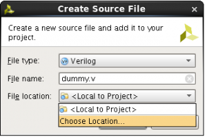
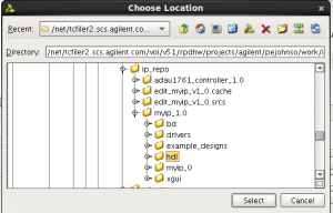
files_fig3Now go to Add Sources again, and after clicking Create File…, specify the file name dummy.v, then select a new file location. files_fig4Navigate to your ip_repo area and into myip_1_0. Select the hdl directory, and click Select. Then click OK and then Finish to create the file. This will place the file in the proper location in the IP repository.

When you merge your changes in the File Groups step, you should not get any warnings. You can then package your IP and use it in your designs.

Hopefully this will be fixed in the next release of Vivado.

Remote JTAG with Vivado

My FPGA development computer is a server in a datacenter. It stores lots of memory and CPU, but it’s impossible to connect it directly to my development boards. ISE has always supported remote JTAG servers, but the implementation has always been spotty. In some releases it has difficulty with some versions of Linux. With Vivado, things are much improved.

If your lab machine is on the same network as your development machine, simply start the hw_server program in the Vivado bin directory and open a target from the development machine Vivado window. Just specify a remote server host name and use the default port 3121. It couldn’t be simpler.

If your lab machine is behind a firewall, you may need to use SSH to tunnel the traffic through. First, make sure the hardware manager is not running on your development machine. From the lab machine, ssh into the development machine with the following command:

ssh -R 3121:localhost:3121 development.my.com

This will create an SSH tunnel from your lab machine to your development machine. If you get a warning saying that SSH can’t bind to the required port it means you are still running a local JTAG server on your development machine. Assuming all went well you should be logged in to your development machine from the lab machine. You can then open the target in the hardware manager in Vivado but tell it to connect to a local machine. Vivido will see a server already running on port 3121 (through your SSH tunnel), so it won’t try to start a new one.

If your lab machine is running Windows then you can use the open source PuTTY program to make the tunnel. If your development machine is running Windows, then you need to install an SSH server on the machine. That’s beyond the scope of this post.

Dual LIFO

The lifo2 module implements a dual Last In First Out stack data structure. The two stack structures share a single block RAM, or may optionally be constructed from shift registers. This module forms the heart of a stack based micro-controller. One of the stacks is used as a data stack while the other is used as a subroutine call stack. By implementing these in a single BRAM we can save a lot of space.

1. Interface

The module interface consists of a clock and reset signal, and a control interface for each stack.

1.1. Module declaration

§1.1.1: §7.1

module lifo2
  §1.3.1. Parameters
  (
   input clk,
   input reset,
   §1.2.1.1. Stack port A,
   §1.2.2.1. Stack port B
   );
      

1.2. Stack ports

The two ports use the suffix a and b to distinguish interface signals. A push input indicates that data from the push_data input should be pushed onto the stack. A pop input indicates that data should be popped from the stack. Popped data should be read from the tos output during the same cycle that pop is valid. It is completely normal to push and pop data on the same clock cycle.

Status signals empty and full indicate if the stack is empty or full. The count output provides the number of valid entries currently on the stack.

1.2.1. Stack port A

§1.2.1.1: §1.1.1

   input push_a,
   input pop_a,
   output reg empty_a,
   output reg full_a,
   output reg `CNT_T count_a,
   output `DATA_T tos_a,
   input `DATA_T push_data_a
	

1.2.2. Stack port B

§1.2.2.1: §1.1.1

   input push_b,
   input pop_b,
   output reg empty_b,
   output reg full_b,
   output reg `CNT_T count_b,
   output `DATA_T tos_b,
   input `DATA_T push_data_b
	

1.3. Parameters

A depth parameter specifies the depth for each of the stacks. For the BRAM implementation, the size of the RAM is just the sum of the two depth parameters. For the shift register implementation each stack uses its depth parameter independently. The width parameter specifies the data width. This is the same for both stacks.

The implementation parameter may be set to "BRAM" or "SRL" to select between BRAM and shift register implementations. Note that the quotes are required.

The full_checking specifies whether the logic that generates the full outputs should be generated. In the case of the shift register implementation the concept of full is easy to implement and sensible. With this implementation, there really are two independent stacks. However, with the BRAM implementation the concept of full is a little harder to pin down. Is the stack full when the number of elements is equal to its depth parameter? This seems overly restrictive since there may still be plenty of room for it to grow. But if it does grow then it does so at the expense of the other stack. There is a further difficulty if both stacks are almost full. If you push to both stacks then you will overflow one of the stacks. Which one? The one that is already over its posted limit? The logic to implement this seems needlessly complex. So the compromise here is to implement the strict full checking for the BRAM implementation when the full_checking parameter is true and to not generate any full checking logic at all if it is false.

§1.3.1: §1.1.1

  #(
    parameter depth_a = 512,
    parameter depth_b = 512,
    parameter width = 32,
    parameter implementation = "SRL",
    parameter full_checking = 0,
    parameter depth = depth_a+depth_b
    )
      

1.4. Definitions

Here are some definitions that we can make use of later. DATA_T is used for data values. PTR_T is used for pointers like the top of stack pointer. The CNT_T definition is suitable for holding a count. Note that this value needs to hold a value of 0 as well as a value of depth so it may be larger than the PTR_T value.

§1.4.1: §7.1

`define DATA_T [width-1:0]
`define PTR_T [log2(depth)-1:0]
`define CNT_T [log2(depth+1)-1:0]
      

2. Functions

The log2 function computes the log base 2 of its input value. This function is used to computer widths of pointer and count values.

§2.1: §7.1

   function integer log2;
      input [31:0] value;
      begin
	 value = value-1;
	 for (log2=0; value>0; log2=log2+1)
	   value = value>>1;
      end
   endfunction
    

3. Logic common to all implementations

3.1. Determine read and write signals

The writing signals indicate that we are writing to the corresponding stack. This occurs when the push signal is asserted and there is space on the stack or if the push signal is asserted and a pop is asserted as well. In this case we can perform the operation even though the stack is full.

The reading signal indicates that we are reading from the corresponding stack. It is just the pop signal qualified with not empty.

§3.1.1: §7.1

  wire writing_a = push_a && (!full_a || pop_a);
  wire writing_b = push_b && (!full_b || pop_b);
  wire reading_a = pop_a && !empty_a;
  wire reading_b = pop_b && ! empty_b;
      

3.2. Determine count value for stack A

We first generate the next_count_a value. Incrementing if we are writing but not reading, decrementing if we are reading and not writing and leaving the count the same if we are both reading and writing or neither reading or writing. We use a separate combinational always block to generate a next value signal next_count_a. This signal is used by later code to determine empty and full conditions.

§3.2.1: §7.1

  reg `CNT_T next_count_a;
  always @(*)
    if (writing_a && !reading_a)
      next_count_a = count_a + 1;
    else if (reading_a && !writing_a)
      next_count_a = count_a - 1;
    else
      next_count_a = count_a;

  always @(posedge clk)
    if (reset)
      count_a <= 0;
    else
      count_a <= next_count_a;
      

3.3. Determine count value for stack B

Here we generate the count values for stack B.

§3.3.1: §7.1

  reg `CNT_T next_count_b;
  always @(*)
    if (writing_b && !reading_b)
      next_count_b = count_b + 1;
    else if (reading_b && !writing_b)
      next_count_b = count_b - 1;
    else
      next_count_b = count_b;
  
  always @(posedge clk)
    if (reset)
      count_a <= 0;
    else
      count_b <= next_count_b;
      

3.4. Generate empty

Here we generate the logic for determining if either stack is empty. The stack is empty if on the next clock its count will be zero.

§3.4.1: §7.1

  always @(posedge clk)
    if (reset)
      empty_a <= 1;
    else
      empty_a <= next_count_a == 0;

  always @(posedge clk)
    if (reset)
      empty_b <= 1;
    else
      empty_b <= next_count_b == 0;
      

3.5. Generate full

Full is pretty simple as well. We go full when the next count value will be equal to the depth parameter of the stack. Writes will not occur when the stack is full so there can never be a case when the next count value is greater than the depth.

§3.5.1: §3.6.1

  always @(posedge clk)
    if (reset)
      full_a <= 0;
    else
      full_a <= next_count_a == depth_a;

  always @(posedge clk)
    if (reset)
      full_b <= 0;
    else
      full_b <= next_count_b == depth_b;
      

3.6. Conditionally generate the full logic

As discussed in Section 1.3, “Parameters”, based on the value of the full_checking parameter we either create the checking logic or just stub the full signals out to always false.

§3.6.1: §7.1

  generate
    if (full_checking)
      begin
        §3.5.1. Generate full
      end
    else
      begin
	initial full_a = 0;
	initial full_b = 0;
      end
  endgenerate
      

4. BRAM implementation

This section describes the BRAM implementation of the dual LIFO.

4.1. The data memory

§4.1.1: §4.6.1

  reg `DATA_T mem [depth-1:0];
      

4.2. Maintain address pointers

Figure 1. The pointer to the top of the A stack grows down while the pointer to the top of the B stack grows up


Here we maintain the address pointers into the RAM. The pointer for stack A starts at address zero and works up, while the pointer for stack B starts at the last address and works down.

§4.2.1: §4.6.1

  wire `PTR_T ptr_a = writing_a ? count_a `PTR_T : (count_a `PTR_T)-1;
  wire `PTR_T ptr_b = (depth-1)-(writing_b ? count_b `PTR_T
                                           : (count_b `PTR_T)-1);
      

4.3. Top-of-stack

One limitation of the BRAM implementation is that we only have two ports. One port must be used for each stack since both stacks can operate simultaneously. The solution to this problem is to recognize that if we are both pushing and popping the stack then we are really only operating on the top element. This element can be stored in a register and no actual memory operation needs to occur.

4.3.1. Top-of-stack shadow registers

The tos_shadow registers hold the latest value pushed onto the stack.

§4.3.1.1: §4.6.1

  reg `DATA_T tos_shadow_a;
  always @(posedge clk)
    if (reset)
      tos_shadow_a <= 0;
    else if (writing_a)
      tos_shadow_a <= push_data_a;

  reg `DATA_T tos_shadow_b;
  always @(posedge clk)
    if (reset)
      tos_shadow_b <= 0;
    else if (writing_b)
      tos_shadow_b <= push_data_b;
	

4.3.2. Select between top-of-stack shadow registers and memory read values

Here we determine if we should use the memory read value or the top-of-stack shadow register to provide the top-of-stack value. If we are popping the stack then the new top-of-stack value should come from the memory read. Otherwise we should just use the value in the top-of-stack shadow register.

§4.3.2.1: §4.6.1

  reg use_mem_rd_a;
  always @(posedge clk)
    if (reset)
      use_mem_rd_a <= 0;
    else if (writing_a)
      use_mem_rd_a <= 0;
    else if (reading_a)
      use_mem_rd_a <= 1;

  reg use_mem_rd_b;
  always @(posedge clk)
    if (reset)
      use_mem_rd_b <= 0;
    else if (writing_b)
      use_mem_rd_b <= 0;
    else if (reading_b)
      use_mem_rd_b <= 1;

  assign tos_a = use_mem_rd_a ? mem_rd_a : tos_shadow_a;

  assign tos_b = use_mem_rd_b ? mem_rd_b : tos_shadow_b;
	

4.4. Perform memory reads

Here we read from the stack. The values read will be the top-of-stack outputs if we are reading from the stack but not writing to it.

§4.4.1: §4.6.1

  reg `DATA_T mem_rd_a;
  always @(posedge clk)
    if (reading_a)
      mem_rd_a <= mem[ptr_a];

  reg `DATA_T mem_rd_b;
  always @(posedge clk)
    if (reading_b)
      mem_rd_b <= mem[ptr_b];
      

4.5. Perform memory writes

Conversely if we are writing to the stack but not reading then we perform a memory write.

§4.5.1: §4.6.1

  always @(posedge clk)
    if (writing_a && !reading_a)
      mem[ptr_a] <= tos_a;

  always @(posedge clk)
    if (writing_b && !reading_b)
      mem[ptr_b] <= tos_b;
      

5. Shift register implementation

5.1. Shift register implementation of stack A

There may be situations where two stacks are needed but we don't want to use a block RAM, or if both stacks don't need to be very large and we want to save the overhead of the RAM implementation. This alternate shift register implementation may be used instead.

The basic idea of the shift register implementation is to use a shift register for each bit of the data word. We then concatenate the head of the shift registers together to form the top of the stack.

5.1.1. Pop data off the shift register

Here we shift the register left, shifting in a zero value.

§5.1.1.1: §5.1.1

srl <= {srl[depth-2:0],1'b0}
	

5.1.2. Push data onto the shift register

Here we shift the push data onto the shift register. This will only happen when the shift register is not full.

§5.1.2.1: §5.1.1

srl <= {push_data_a[i],srl[depth_a-1:1]}
	

5.1.3. Swap data at the top of the shift register

Here we just replace the leftmost value in the shift register with the new pushed value.

§5.1.3.1: §5.1.1

srl <= {push_data_a[i],srl[depth_a-2:0]}
	

We use a generate for loop to implement each shift register and a case statement to update it based on the push and pop conditions.

§5.1.1: §5.1

for (i=0; i<width; i=i+1)
  begin : srl_a
    reg [depth_a-1:0] srl;
    always @(posedge clk)
      case ({writing_a,reading_a})
	2'b01: §5.1.1.1. Pop data off the shift register;
	2'b10: §5.1.2.1. Push data onto the shift register;
	2'b11: §5.1.3.1. Swap data at the top of the shift register;
      endcase

      assign tos_a[i] = srl[depth_a-1];
  end
      

5.2. Shift register implementation of stack B

The implementation for stack B is the same as for stack A but with the appropriate name changes.

§5.2.1: §5.1

for (i=0; i<width; i=i+1)
  begin : srl_b
    reg [depth_b-1:0] srl;
    always @(posedge clk)
      case ({writing_b,reading_b})
	2'b01: srl <= {srl[depth_b-2:0],1'b0};
	2'b10: srl <= {push_data_b[i],srl[depth_b-1:1]};
	2'b11: srl <= {push_data_b[i],srl[depth_b-2:0]};
      endcase
      assign tos_b[i] = srl[depth_b-1];
  end
      

For the shift register implementation we just declare the generate loop variable and then instantiate the two stacks.

6. Undefined implementation

§6.1: §7.1

	initial
	  begin
	    $display("***ERROR: %m: Undefined implementation \"%0s\".",implementation);
	    $finish;
	  end
    

7. The main module

This is where we tie everything together.

§7.1

§1.1. Header
§2.1. Copyright

`timescale 1ns/1ns
§1.4.1. Definitions

§1.1.1. Module declaration

§2.1. Functions

§3.1.1. Determine read and write signals

§3.2.1. Determine count value for stack A
§3.3.1. Determine count value for stack B

§3.4.1. Generate empty
§3.6.1. Conditionally generate the full logic

`ifndef SYNTHESIS
   initial
     $display("***INFO: %m: lifo2.v implementation=\"%0s\".",implementation);
`endif
  generate
    if (implementation == "BRAM")
      begin : bram_implementation
        §4.6.1. BRAM implementation body
      end
    else if (implementation == "SRL")
      begin : srl_implementation
        §5.1. Shift register implementation
      end
    else
      begin
        §6.1. Undefined implementation
      end
  endgenerate
endmodule
    

A. Front matter

1. Header

§1.1: §7.1

//-----------------------------------------------------------------------------
// Title         : Dual LIFO stack
// Project       : Common
//-----------------------------------------------------------------------------
// File          : lifo2.v
//-----------------------------------------------------------------------------
// Description :
// 
// Two Synchronous LIFO stacks using a single BRAM.
//
// The stacks start at each end and grow to the middle.
//
      

2. Copyright

§2.1: §7.1

//-----------------------------------------------------------------------------
// Copyright 2009 Beyond Circuits. All rights reserved.
//
// Redistribution and use in source and binary forms, with or without modification,
// are permitted provided that the following conditions are met:
//   1. Redistributions of source code must retain the above copyright notice, 
//      this list of conditions and the following disclaimer.
//   2. Redistributions in binary form must reproduce the above copyright notice, 
//      this list of conditions and the following disclaimer in the documentation 
//      and/or other materials provided with the distribution.
//
// THIS SOFTWARE IS PROVIDED BY THE BEYOND CIRCUITS ``AS IS'' AND ANY EXPRESS OR 
// IMPLIED WARRANTIES, INCLUDING, BUT NOT LIMITED TO, THE IMPLIED WARRANTIES OF 
// MERCHANTABILITY AND FITNESS FOR A PARTICULAR PURPOSE ARE DISCLAIMED. IN NO EVENT 
// SHALL BEYOND CIRCUITS BE LIABLE FOR ANY DIRECT, INDIRECT, INCIDENTAL, SPECIAL,
// EXEMPLARY, OR CONSEQUENTIAL DAMAGES (INCLUDING, BUT NOT LIMITED TO, PROCUREMENT
// OF SUBSTITUTE GOODS OR SERVICES; LOSS OF USE, DATA, OR PROFITS; OR BUSINESS 
// INTERRUPTION) HOWEVER CAUSED AND ON ANY THEORY OF LIABILITY, WHETHER IN CONTRACT, 
// STRICT LIABILITY, OR TORT (INCLUDING NEGLIGENCE OR OTHERWISE) ARISING IN ANY WAY 
// OUT OF THE USE OF THIS SOFTWARE, EVEN IF ADVISED OF THE POSSIBILITY OF SUCH DAMAGE.
//------------------------------------------------------------------------------
      

B. Downloads

The Verilog code for lifo2.v can be downloaded here. Since this post is so long I have also included a link the article in PDF form here.

Verilog functions in Xilinx XST

A nice idea

The XST documentation says that Verilog functions are fully supported. I was frustrated today to discover that this is not the case. I was trying to make a library for handling fixed point arithmetic. Module instantiation overhead in Verilog is quite high in terms of lines of code and excess verbiage. All the code I need to use is combinational, so the natural thing to do is have one module with all my functions and parameters which control the representation of the fixed point numbers. After this, I can make instances of the library module with the various fixed point representations I need and use the functions.

So I whip out the following:


module SignedInteger
    parameter out_int = 1;
    parameter out_frac = 1;
    parameter in_a_int = out_int;
    parameter in_a_frac = out_frac;
    parameter in_b_int = in_a_int;
    parameter in_b_frac = in_a_frac;
    parameter out_width = out_int+out_frac;
    parameter in_a_width = in_a_int+in_a_frac;
    parameter in_b_width = in_b_int+in_b_frac;

    function signed [out_width-1:0] sum;
    input signed [in_a_width-1:0] a;
    input signed [in_b_width-1:0] b;
    begin
      if (in_a_frac > in_b_frac)
	sum = a + (b<<(in_a_frac-in_b_frac));
      else
	sum = (a<<(in_b_frac-in_a_frac)) + b;
    end
  endfunction

endmodule

Now I can instantiate SignedInteger in another module and call the sum function. I need the function in another module because I may have multiple instances of SignedInteger in the calling module with different parameter values– sort of a poor man’s class mechanism. Everything simulates just peachy. Now, I synthesize a test case in XST.

Prepare to crash and burn

I’ll spare you the details, but XST has a number of issues with doing things like this, though the first few are not insurmountable. XST will first error out because I used concatenation instead of shift operators in the sum function. XST didn’t like the fact that one of the concatenation multipliers was negative. I got boxed into a corner here by Verilog too, because you can’t use a generate inside a function, and if I use a generate outside the function, it makes it really hard to call the function from outside the module. So, we’ll go back to the drawing board and use the shift operator. Next, XST believes that modules need at least one port. My guess is that the people who wrote XST never thought about just using a module as a container for its tasks and functions. Hmm… it’s not great, but I can add a port that I won’t use.

At this point, I’m faced with an interesting error message:


Analyzing top module .
ERROR:Xst:917 - Undeclared signal .
ERROR:Xst:2083 - "test.v" line 29: Unsupported range for function.

What do you mean, undeclared signal out_width? Firstly, it’s not a signal and secondly, it is so declared. The second message gives me pause. Crap– it really thinks that out_width is a signal. Why can’t it see it?

An experiment

Time for a test case. I try to synthesize this module, and guess what? It compiles without errors.


module test2
  (
   input signed [15:0] a,
   input signed [15:0] b,
   output signed [19:0] sum
   );

  localparam out_width = 20;
  localparam in_a_width = 16;
  localparam in_a_frac = 0;
  localparam in_b_width = 16;
  localparam in_b_frac = 4;

  SignedInteger #(16,4,16,0,12,4) si_16_4_16_0_12_4(.value());

  assign sum = si_16_4_16_0_12_4.sum(a,b);
endmodule

If I give it the parameters it is looking for, the errors go away. I do get some strange warnings, however…


WARNING:Xst:616 - Invalid property "out_width 00000014": Did not attach to si_16_4_16_0_12_4.
WARNING:Xst:616 - Invalid property "in_a_frac 00000000": Did not attach to si_16_4_16_0_12_4.
WARNING:Xst:616 - Invalid property "in_a_int 00000010": Did not attach to si_16_4_16_0_12_4.
WARNING:Xst:616 - Invalid property "in_a_width 00000010": Did not attach to si_16_4_16_0_12_4.
WARNING:Xst:616 - Invalid property "in_b_frac 00000004": Did not attach to si_16_4_16_0_12_4.
WARNING:Xst:616 - Invalid property "in_b_int 0000000C": Did not attach to si_16_4_16_0_12_4.
WARNING:Xst:616 - Invalid property "in_b_width 00000010": Did not attach to si_16_4_16_0_12_4.
WARNING:Xst:616 - Invalid property "out_frac 00000004": Did not attach to si_16_4_16_0_12_4.
WARNING:Xst:616 - Invalid property "out_int 00000010": Did not attach to si_16_4_16_0_12_4.

Not sure what that means exactly, but it sounds like something is rotten with the parameters.

Incorrect logic

Now this could cause incorrect logic to be synthesized. So I tried this test case.


module sub(empty);
  output empty;
  parameter paramvalue = 1;

  assign empty = 0;
  function [3:0] myparam_plus;
    input [3:0] in;
    begin
      myparam_plus = paramvalue + in;
    end
  endfunction
endmodule // sub

module test3(value,empty);
  output [3:0] value;
  output empty;
  parameter paramvalue = 10;
  sub #(2) mysub(.empty(empty));
  assign value = mysub.myparam_plus(3);
endmodule

The value output is a constant 5. That is, the sub module has a paramvalue of 2 and we add 3 to it. XST synthesizes this with no errors, warnings, or infos. The module is totally clean. Even so, the netlist it produces gives value a constant output of 13. Let’s see Xilinx support try to squirm their way out of this one. This seems like a bug to me.

At any rate, I have to give up on a pure Verilog solution to a fixed point library. Time to use Perl.